 | –≠–ª–µ–∫—Ç—Ä–æ–Ω–Ω—ã–π –∫–æ–º–ø–æ–Ω–µ–Ω—Ç: C9950 | –°–∫–∞—á–∞—Ç—å:  PDF PDF  ZIP ZIP |
3.3V, 180-MHz, Multi-Output Clock Driver
C9950
Cypress Semiconductor Corporation
∑
3901 North First Street
∑
San Jose
∑
CA 95134
∑
408-943-2600
Document #: 38-07072 Rev. *C
Revised December 21, 2002
Product Features
∑ 180-MHz Clock Support
∑ Supports PowerPCTM, Intel
Æ
, and RISC Processors
∑ 9 Clock Outputs: Frequency Configurable
∑ Oscillator or Crystal Reference Input
∑ Output Disable Control
∑ Spread Spectrum Compatible
∑ Pin Compatible with MPC950
∑ Industrial Temp. Range: ≠40∞C to +85∞C
∑ 32-Pin TQFP Package
Note:
1.
x = is the reference input frequency
Table 1. Frequency Table
[1]
SEL
(A:D)
FB_SEL = 1
FB_SEL = 1
QA
QB
QC
(0,1)
QD
(0:4)
QA
QB
QC
(0,1)
QD
(0:4)
0000
4x
2x
2x
2x
8x
4x
4x
4x
0001
4x
2x
2x
x
8x
4x
4x
2x
0010
4x
2x
x
2x
8x
4x
2x
4x
0011
4x
2x
x
x
8x
4x
2x
2x
0100
4x
x
2x
2x
8x
2x
4x
4x
0101
4x
x
2x
x
8x
2x
4x
2x
0110
4x
x
x
2x
8x
2x
2x
4x
0111
4x
x
x
x
8x
2x
2x
2x
1000
2x
2x
2x
2x
4x
4x
4x
4x
1001
2x
2x
2x
x
4x
4x
4x
2x
1010
2x
2x
x
2x
4x
4x
2x
4x
1011
2x
2x
x
x
4x
4x
2x
2x
1100
2x
x
2x
2x
4x
2x
4x
4x
1101
2x
x
2x
x
4x
2x
4x
2x
1110
2x
x
x
2x
4x
2x
2x
4x
1111
2x
x
x
x
4x
2x
2x
2x
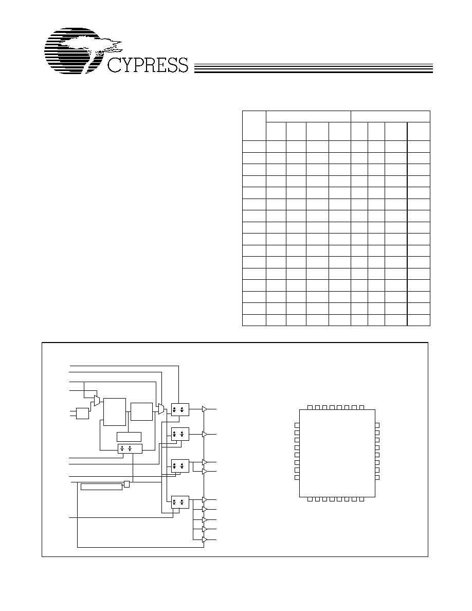
Block Diagram
Pin Configuration
OSC
Phase
Detector
VCO
200-
480MHz
LPF
8/ 16
2/ 4
4/ 8
4/ 8
4/ 8
QA
QB
QC0
QC1
QD0
QD1
QD2
QD3
QD4
SELA
PLL_EN
TCLK
REF_SEL
XIN
XOUT
FB_SEL
SELB
SELC
MR/OE#
Power-On Reset
SELD
C9950
REF
_
SEL
P
LL_E
N
TC
L
K
VSS
QA
VDDC
QB
VSS
XO
UT
MR
/OE#
VDDC
QD
4
VSS
QD
3
VDDC
QD
2
QC0
VDDC
QC1
VSS
QD0
VDDC
QD1
VSS
VDD
FB_SEL
SELA
SELB
SELC
SELD
VSS
XIN
1
2
3
4
5
6
7
8
24
23
22
21
20
19
18
17
9
10
11
12
13
14
15
16
32
31
30
29
28
27
26
25

C9950
Document #: 38-07072 Rev. *C
Page 2 of 7
Note:
2.
PD = Internal Pull-Down, PU = Internal Pull-Up.
Pin Description
[2]
Pin Name
PWR
I/O
Type
Description
8
XIN
I
Oscillator Input. Connect to a crystal.
9
XOUT
0
Oscillator Output. Connect to a crystal.
30
TCLK
I
External Test Clock Input.
28
QA
VDDC
O
Clock Output. See Frequency Table.
26
QB
VDDC
O
Clock Output. See Frequency Table.
22, 24
QC(1,0)
VDDC
O
Clock Outputs. See Frequency Table.
12, 14, 16, 18, 20
QD(4:0)
VDDC
O
Clock Outputs. See Frequency Table.
2
FB_SEL
I
PD
Feedback Select Input.
If FB_SEL = 1, then the (
˜
8) counter is selected in the PLL feed-
back loop.
If FB_SEL = 0, then the (
˜
16) counter is selected in the PLL
feedback loop.
10
MR/OE#
I
Master Reset/Output Enable Input. When asserted HIGH, resets
all of the internal flip-flops and also disables all of the outputs.
When pulled LOW, releases the internal flip-flops from reset and
enables all of the outputs.
31
PLL_EN
I
PLL Enable Input. When asserted HIGH, PLL is enabled. And
when set LOW, PLL is bypassed.
32
REF_SEL
I
Reference Select Input. When HIGH, TCLK is the reference clock
and when LOW, the crystal oscillator is selected.
3, 4, 5, 6
SEL(A:D)
I
Frequency Select Inputs. See Frequency Table.
If SEL_ = 1, then QA divider =
˜
4, QB:D divider =
˜
8
If SEL_ = 0, then QA divider =
˜
2, QB:D divider =
˜
4
11, 15, 19, 23, 27
VDDC
3.3V Power Supply for Output Clock Buffers.
1
VDD
3.3V Power Supply for PLL
7, 13, 17, 21, 25,
29
VSS
Common Ground

C9950
Document #: 38-07072 Rev. *C
Page 3 of 7
Description
The C9950 has an integrated PLL that provides low skew and
low jitter clock outputs for high-performance microprocessors.
The PLL is ensured stable operation given that the VCO is
configured to run between 200 MHz and 480 MHz. This allows
a wide range of output frequencies from 25 MHz to 180 MHz.
The internal VCO frequency is divided by 8 or 16 and com-
pared to the input reference clock. These selectable dividers
allow for input reference clock flexibility. The internal VCO is
running at 2x or 4x the high speed output (QA), and 4x or 8x
the outputs Q(B:D) depending on the configuration (see Table
2). The use of even dividers ensures that the output duty cycle
remains at 50%.
Output Frequency
The C9950 generates outputs with programmable frequency
relationships. As a result, the input reference frequency is a
function of the desired output frequency (Table 1). The follow-
ing block diagram illustrates the corresponding parameters
that are needed to calculate the output frequency.
Fref = FVCO/m, FVCO = FQn x N
Fref = (FQn x N) / m
Where m = 8 (FB_SEL = 1) or m = 16 (FB_SEL = 0), and N = 2, 4, or 8 depending on SEL_ as shown in Table 1.
Phase
Detector
VCO
LPF
/m
/N
Fref
Qn
Figure 1.
Table 2.
INPUTS
OUTPUTS
SELA
SELB
SELC
SELD
QA
QB
QC
QD
0
0
0
0
VCO/2
VCO/4
VCO/4
VCO/4
0
0
0
1
VCO/2
VCO/4
VCO/4
VCO/8
0
0
1
0
VCO/2
VCO/4
VCO/8
VCO/4
0
0
1
1
VCO/2
VCO/4
VCO/8
VCO/8
0
1
0
0
VCO/2
VCO/8
VCO/4
VCO/4
0
1
0
1
VCO/2
VCO/8
VCO/4
VCO/8
0
1
1
0
VCO/2
VCO/8
VCO/8
VCO/4
0
1
1
1
VCO/2
VCO/8
VCO/8
VCO/8
1
0
0
0
VCO/4
VCO/4
VCO/4
VCO/4
1
0
0
1
VCO/4
VCO/4
VCO/4
VCO/8
1
0
1
0
VCO/4
VCO/4
VCO/8
VCO/4
1
0
1
1
VCO/4
VCO/4
VCO/8
VCO/8
1
1
0
0
VCO/4
VCO/8
VCO/4
VCO/4
1
1
0
1
VCO/4
VCO/8
VCO/4
VCO/8
1
1
1
0
VCO/4
VCO/8
VCO/8
VCO/4
1
1
1
1
VCO/4
VCO/8
VCO/8
VCO/8

C9950
Document #: 38-07072 Rev. *C
Page 4 of 7
Notes:
3.
For best performance and accurate frequencies from this device, It is recommended but not mandatory that the chosen crystal meets or exceeds these
specifications
4.
Larger values may cause this device to exhibit oscillator startup problems
Table 3. Suggested Oscillator Crystal Parameters
Parameter
Description
Conditions
Min.
Typ.
Max.
Unit
T
C
Frequency Tolerance
Note 1
-
-
±100
PPM
T
S
Frequency Temperature
Stability
(T
A
≠10 to +60∞C)
[3]
-
-
±100
PPM
T
A
Aging
(first 3 years @ 25∞C)
[3]
-
-
5
PPM/Yr
C
L
Load Capacitance
The crystal's rated load
[3]
-
20
-
pF
R
ESR
Effective Series
Resistance (ESR)
Note 4
-
40
80
Ohms

C9950
Document #: 38-07072 Rev. *C
Page 5 of 7
Maximum Ratings
[5]
Maximum Input Voltage Relative to V
SS
: ............ V
SS
≠ 0.3V
Maximum Input Voltage Relative to V
DD
: ............. V
DD
+ 0.3V
Storage Temperature: ................................≠65∞C to + 150∞C
Operating Temperature: ................................ ≠40∞C to +85∞C
Maximum ESD protection .............................................. 2 KV
Maximum Power Supply: ................................................5.5V
Maximum Input Current:
..................................................±
20 mA
This device contains circuitry to protect the inputs against
damage due to high static voltages or electric field; however,
precautions should be taken to avoid application of any volt-
age higher than the maximum rated voltages to this circuit. For
proper operation, V
in
and V
out
should be constrained to the
range:
V
SS
< (V
in
or V
out
) < V
DD
Unused inputs must always be tied to an appropriate logic volt-
age level (either V
SS
or V
DD
).
Notes:
5.
The voltage on any input or I/O pin cannot exceed the power pin during power-up. Power supply sequencing is NOT required.
6.
Inputs have internal pull-up/pull-down resistors that affect input current.
7.
Driving series or parallel terminated 50
(or 50
to V
DD
/2) transmission. Output buffers are dual staged to control drive strength in order to reduce over / under
shoot.
8.
Parameters are guaranteed by design and characterization. Not 100% tested in production.
9.
Maximum and minimum input reference is limited by the VCO lock range.
10. Outputs loaded with 30 pF each.
DC Parameters:
V
DD
= V
DDC
= 3.3V ±5%, T
A
= ≠40∞C to +85∞C
Parameter
Description
Conditions
Min.
Typ.
Max.
Unit
V
IL
Input Low Voltage
0.8
V
V
IH
Input High Voltage
2.0
V
I
IL
Input Low Current (@V
IL
= V
SS
)
Note 6
≠120
µA
I
IH
Input High Current (@V
IL
=V
DD
)
Note 6
120
µA
V
OL
Output Low Voltage
I
OL
= 40 mA, Note 7
0.5
V
V
OH
Output High Voltage
I
OH
= ≠40 mA, Note 7
2.4
V
I
DDC
Quiescent Supply Current
All V
DDC
and V
DD
15
20
mA
I
DD
PLL Supply Current
V
DD
only
15
20
mA
C
in
Input Capacitance
4
pF
AC Parameters
[8]
:
V
DD
= V
DDC
= 3.3V ±5%, T
A
= ≠40∞C to +85∞C
Parameter
Description
Conditions
Min.
Typ.
Max.
Unit
Tr/Tf
TCLK Input Rise/Fall
3.0
ns
Fref
Reference Input Frequency
Note 9
Note 2
MHz
Fxtal
Crystal Oscillator Frequency
See Table 3 for details
10
25
MHz
FrefDC
Reference Input Duty Cycle
25
75
%
Fvco
PLL VCO Lock Range
200
480
MHz
Tlock
Maximum PLL lock Time
10
ms
Tr/Tf
Output Clocks Rise/Fall Time
[10]
0.8V to 2.0V
0.10
1.0
ns
Fout
Maximum Output Frequency
QA = (
˜
2)
180
MHz
QA/QB = (
˜
4)
120
QB = (
˜
8)
60
FoutDC
Output Duty Cycle
TCYCLE/2 ≠ 1
TCYCLE/2 + 1
ns
tpZL, tpZH
Output enable time (all outputs)
6
ns
tpLZ, tpHZ
Output disable time (all outputs)
7
ns
TCCJ
Cycle to Cycle Jitter (peak to peak)
[10]
±100
ps
TSKEW0
Any Output to Any Output Skew
[10]
200
350
ps