 | ÐлекÑÑоннÑй компоненÑ: CG6235AS | СкаÑаÑÑ:  PDF PDF  ZIP ZIP |
38-07624.fm
MPEG Clock Generator with VCXO
CG6235AS
Cypress Semiconductor Corporation
·
3901 North First Street
·
San Jose
,
CA 95134
·
408-943-2600
Document #: 38-07624 Rev. *B
Revised February 10, 2004
Features
· Integrated phase-locked loop (PLL)
· Low-jitter, high-accuracy outputs
· VCXO with analog adjust
· 3.3V operation
Benefits
· Highest-performance PLL tailored for multimedia applica-
tions
· Meets critical timing requirements in complex system
designs
· Application compatibility for a wide variety of designs
Frequency Table
Part Number Outputs
Input Frequency Range
Output Frequencies
VCXO Control
Curve
Other Features
CG6235AS
1
27-MHz pullable crystal input
per Cypress specification
One copy of 27 MHz
One copy of 83.33 MHz
(non-pullable)
linear
Pinout compatible with MK3741
27
XIN
XOUT
OSC
VCXO
VDD
VSS
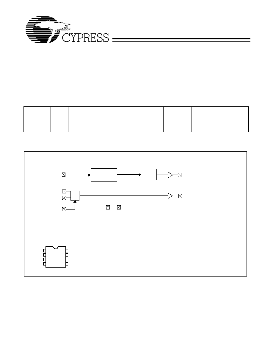
Block Diagram
8-pin SOIC
CG6235AS
1
2
3
4
XOUT
XIN
VCXO
XBUF/27 MHz
VSS
REF
83.33 MHz
5
6
7
8
VDD
Pin Configuration
OUTPUT
DIVIDER
PLL
83.33MHz
XBUF/27MHz
54 REF
CG6235AS
Document #: 38-07624 Rev. *B
Page 2 of 6
Pin Descriptions
Name
Pin Number
Description
XIN
1
Reference crystal input.
VDD
2
Voltage supply.
VCXO
3
Input analog control for VCXO.
VSS
4
Ground.
XBUF/27 MHz 5
27-MHz buffered crystal output.
83.33 MHz
6
83.33-MHz clock output.
REF
7
54-MHz reference input.
XOUT
8
Reference crystal output.
CG6235AS
Document #: 38-07624 Rev. *B
Page 3 of 6
Absolute Maximum Conditions
Supply Voltage (V
DD
) ........................................0.5 to +7.0V
DC Input Voltage...................................... 0.5V to V
DD
+ 0.5
Storage Temperature (Non-condensing).....55
°C to +125°C
Junction Temperature ................................ 40
°C to +125°C
Data Retention @ Tj = 125
°C................................> 10 years
Package Power Dissipation...................................... 350 mW
ESD (Human Body Model) MIL-STD-883................. > 2000V
(Above which the useful life may be impaired. For user guide-
lines, not tested.)
Pullable Crystal Specifications
[1]
Parameter
Description
Comments
Min. Typ. Max.
Unit
F
NOM
Nominal crystal frequency
Parallel resonance, fundamental mode, AT
cut
27
MHz
C
LNOM
Nominal load capacitance
14
pF
R
1
Equivalent series resistance (ESR)
Fundamental mode
25
R
3
/R
1
Ratio of third overtone mode ESR to
fundamental mode ESR
Ratio used because typical R
1
values are
much less than the maximum spec
3
DL
Crystal drive level
No external series resistor assumed
150
µW
F
3SEPHI
Third overtone separation from 3*F
NOM
High side
300
ppm
F
3SEPLO
Third overtone separation from 3*F
NOM
Low side
150
ppm
C
0
Crystal shunt capacitance
7
pF
C
0
/C
1
Ratio of shunt to motional capacitance
180
250
C
1
Crystal motional capacitance
14.4
18
21.6
fF
Recommended Operating Conditions
Parameter
Description
Min.
Typ.
Max.
Unit
V
DD
Operating Voltage
3.135
3.3
3.465
V
T
A
Ambient Temperature
0
70
°C
C
LOAD
Max. Load Capacitance
15
pF
t
PU
Power-up time for all V
DD
pins to reach minimum specified
voltage (power ramps must be monotonic)
0.05
500
ms
DC Electrical Specifications
Parameter
Name
Description
Min.
Typ.
Max.
Unit
I
OH
Output HIGH Current
V
OH
= V
DD
0.5V, V
DD
= 3.3V
12
24
mA
I
OL
Output LOW Current
V
OL
= 0.5V, V
DD
= 3.3V
12
24
mA
C
IN
Input Capacitance
Except XIN, XOUT pins
7
pF
V
VCXO
VCXO Input Range
0
V
DD
V
f
XO
[2]
VCXO Pullability Range
75/175
ppm
I
VDD
Supply Current
40
mA
AC Electrical Specifications
(V
DD
= 3.3V)
[3]
Parameter
[3]
Name
Description
Min.
Typ.
Max.
Unit
DC
Output Duty Cycle
Duty Cycle is defined in Figure 1, 50% of V
DD
45
50
55
%
ER
Rising Edge Rate
Output Clock Edge Rate, Measured from 20%
to 80% of V
DD
, C
LOAD
= 15 pF. See Figure 2.
0.8
1.4
V/ns
EF
Falling Edge Rate
Output Clock Edge Rate, Measured from 80%
to 20% of V
DD
, C
LOAD
= 15 pF. See Figure 2.
0.8
1.4
V/ns
t
9
Clock Jitter 83.33 MHz
Peak-to-peak period jitter
500
ps
Notes:
1.
Crystals that meet this specification includes: Ecliptek ECX-5788-13.500M,Siward XTL001050A-13.5-14-400, Raltron A-13.500-14-CL,PDI
HA13500XFSA14XC.
2.
75/+175 ppm assumes 2.5 pF of additional board level load capacitance. This range will be shifted down with less board capacitance or shifted up with more
board capacitance.
3.
Not 100% tested.
CG6235AS
Document #: 38-07624 Rev. *B
Page 4 of 6
Voltage and Timing Definitions
t
9
Clock Jitter XBUF/27 MHz
Peak-to-peak period jitter
375
ps
t
10
PLL Lock Time
3
ms
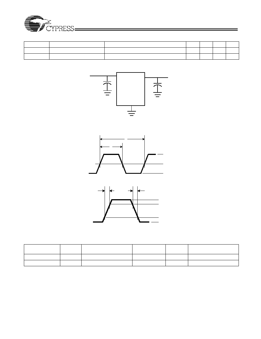
Test and Measurement Set-up
AC Electrical Specifications
(V
DD
= 3.3V) (continued)
[3]
Parameter
[3]
Name
Description
Min.
Typ.
Max.
Unit
0.1
µF
VDD
Outputs
C
LOAD
GND
DUT
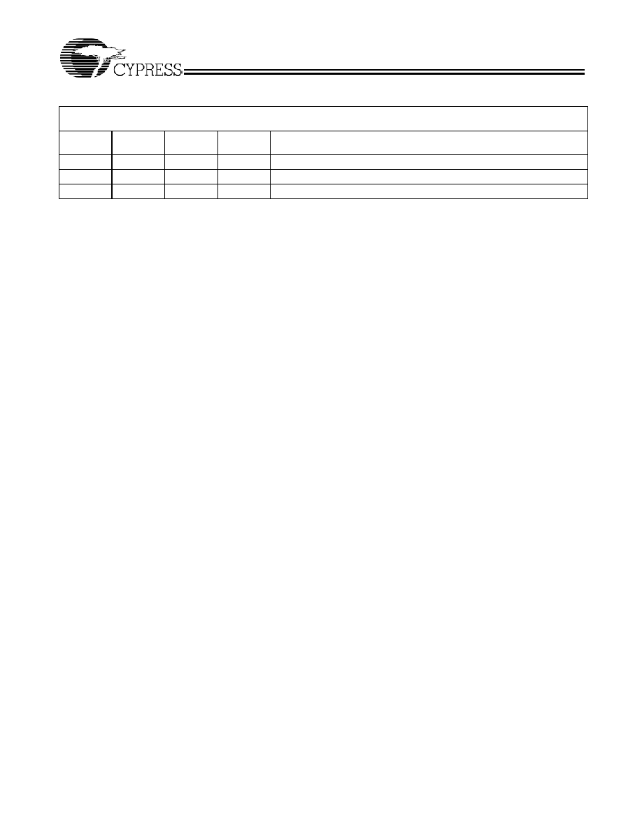
Ordering Information
Ordering Code
Package
Name
Package Type
Operating Range
Operating
Voltage
Features
CG6235AS
S8
8-pin SOIC
Commercial
3.3V
Linear VCXO control curve
CG6235AST
S8
8-pin SOIC Tape and Reel Commercial
3.3V
Linear VCXO control curve
Clock
Output
V
DD
50% of V
DD
0V
t
1
t
2
Figure 1. Duty Cycle Definition
Clock
Output
t
3
t
4
V
DD
80% of V
DD
20% of V
DD
0V
Figure 2. ER = (0.6 x V
DD
) /t3, EF = (0.6 x V
DD
) /t4
CG6235AS
Document #: 38-07624 Rev. *B
Page 5 of 6
© Cypress Semiconductor Corporation, 2004. The information contained herein is subject to change without notice. Cypress Semiconductor Corporation assumes no responsibility for the use
of any circuitry other than circuitry embodied in a Cypress Semiconductor product. Nor does it convey or imply any license under patent or other rights. Cypress Semiconductor does not authorize
its products for use as critical components in life-support systems where a malfunction or failure may reasonably be expected to result in significant injury to the user. The inclusion of Cypress
Semiconductor products in life-support systems application implies that the manufacturer assumes all risk of such use and in doing so indemnifies Cypress Semiconductor against all charges.
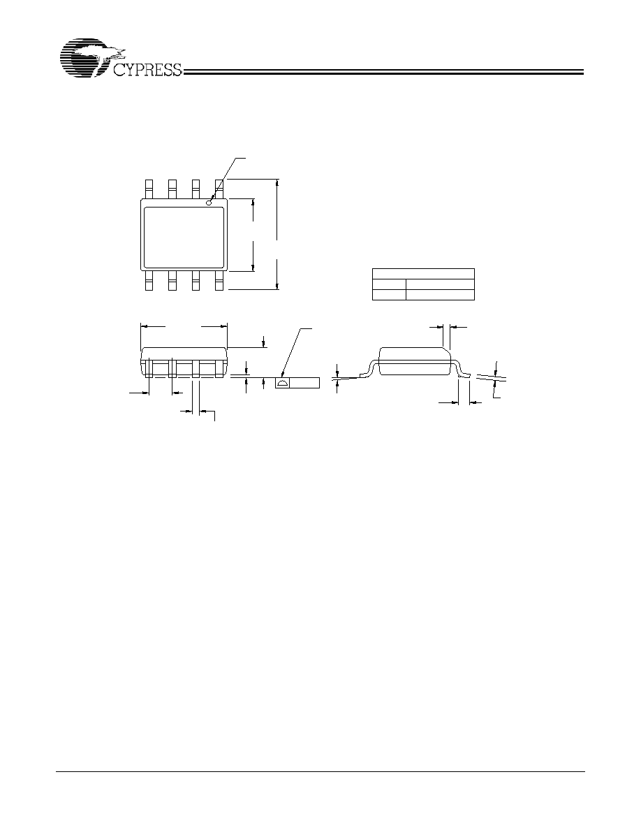
Package Drawing and Dimensions
All product or company names mentioned in this document may be the trademarks of their respective holders.
SEATING PLANE
PIN 1 ID
0.230[5.842]
0.244[6.197]
0.157[3.987]
0.150[3.810]
0.189[4.800]
0.196[4.978]
0.050[1.270]
BSC
0.061[1.549]
0.068[1.727]
0.004[0.102]
0.0098[0.249]
0.0138[0.350]
0.0192[0.487]
0.016[0.406]
0.035[0.889]
0.0075[0.190]
0.0098[0.249]
1. DIMENSIONS IN INCHES[MM] MIN.
MAX.
0°~8°
0.016[0.406]
0.010[0.254]
X 45°
2. PIN 1 ID IS OPTIONAL,
ROUND ON SINGLE LEADFRAME
RECTANGULAR ON MATRIX LEADFRAME
0.004[0.102]
8 Lead (150 Mil) SOIC - S08
1
4
5
8
3. REFERENCE JEDEC MS-012
PART #
S08.15 STANDARD PKG.
SZ08.15 LEAD FREE PKG.
4. PACKAGE WEIGHT 0.07gms
8-lead (150-Mil) SOIC S8
51-85066-*C
CG6235AS
Document #: 38-07624 Rev. *B
Page 6 of 6
Document History Page
Document Title: CG6235AS MPEG Clock Generator with VCXO
Document Number: 38-07624
REV.
ECN NO. Issue Date
Orig. of
Change
Description of Change
**
131682
01/09/04
RGL
New Data Sheet
*A
132862
01/15/04
RGL
Minor Change: Post to external website
*B
204043
See ECN
RGL
Minor Change: Fixed the block diagram (aligned labels with the blocks)