/home/web/htmldatasheet/RUSSIAN/html/cypress/169216
High - Accuracy EPROM Programmable
PLL Die for Crystal Oscillators
CY2037
Cypress Semiconductor Corporation
·
3901 North First Street
·
San Jose
·
CA 95134
·
408-943-2600
Document #: 38-07354 Rev. *A
Revised December 7, 2002
Features
Benefits
· EPROM-programmable die for in-package program-
ming of crystal oscillators
Enables quick turnaround of custom oscillators
Lowers inventory costs through stocking of blank parts
· High resolution PLL with 12 bit multiplier and 10 bit di-
vider
Enables synthesis of highly accurate and stable output clock
frequencies with zero or low PPM
· EPROM-programmable capacitor tuning array with
Shadow register
Enables fine-tuning of output clock frequency by adjusting
C
Load
of the crystal
· Twice programmable die (CY2037A and CY2037-2).
Enables reprogramming of programmed part, to correct errors,
and control excess inventory
· Simple 4-wire programming interface
Enables programming of output frequency after packaging
· On-chip oscillator runs from 1030 MHz fundamental
tuned crystal
Lowers cost of oscillator as PLL can be programmed to a high
frequency using a low-frequency, low-cost crystal
· EPROM-selectable TTL or CMOS duty cycle levels
Duty cycle centered at 1.4V or V
DD
/2
Provides flexibility to service most TTL or CMOS applications
· Operating frequency
-- 1133 MHz at 5V
-- 1100 MHz at 3.3V
-- 166.6 MHz at 2.7V
Services most PC, networking, and consumer applications
· Sixteen selectable post-divide options, using either
PLL or reference oscillator output
Provides flexibility in output configurations and testing
· Programmable PWR_DWN or OE pin (CY2037A and
CY2037-2)
· Frequency Select (CY2037-3)
Enables low-power operation or output enable function
Enables two frequency options for meeting different industry
standards, i.e., PAL/NTSC.
· Programmable asynchronous or synchronous OE and
PWR_DWN modes (CY2037 and CY2037-2)
Provides flexibility for system applications, through selectable
instantaneous or synchronous change in outputs
· Low Jitter outputs typically
-- < ± 100 ps (pk-pk) at 5V and f>33 MHz
-- < ± 125 ps (pk-pk) at 3.3V and f>33 MHz
Suitable for most PC, consumer, and networking applications
· 3.3V or 5V operation
Lowers inventory cost as same die services both applications
· Small Die
Enables encapsulation in small-size, surface mount packages
· Controlled rise and fall times and output slew rate
Has lower EMI than oscillators
CY2037
Document #: 38-07354 Rev. *A
Page 2 of 9
Functional Description
The CY2037 is an EPROM programmable, high accuracy,
PLL-based die designed for the crystal oscillator market. The
die attaches directly to a low-cost 1030 MHz crystal and can
be packaged into 4-pin through-hole or surface mount pack-
ages. The oscillator devices can be stocked as blank parts and
custom frequencies programmed in-package at the last stage
before shipping. This enables fast-turn manufacture of custom
and standard crystal oscillators without the need for dedicated,
expensive crystals.
The CY2037 contains an on-chip oscillator and an unique os-
cillator tuning circuit for fine-tuning of the output frequency.
The crystal C
load
can be selectively adjusted by programming
a set of seven EPROM bits. This feature can be used to com-
pensate for crystal variations or to obtain a more accurate syn-
thesized frequency.
The CY2037 uses EPROM programming with a simple 2-wire,
4-pin interface that includes V
SS
and V
DD
. Clock outputs can
be generated up to 133 MHz at 5V or up to 100 MHz at 3.3V.
The entire configuration can be reprogrammed one time, al-
lowing programmed inventory to be altered or reused.
The CY2037 PLL die has been designed for very high resolu-
tion. It has a 12 bit feedback counter multiplier and a 10 bit
reference counter divider. This enables the synthesis of highly
accurate and stable output clock frequencies with zero or low
PPM error. The clock can be further modified by eight output
divider options of 1, 2, 4, 8, 16, 32, 64, and 128. The divider
input can be selected as either the PLL or crystal oscillator
output providing a total of sixteen separate output options. For
further flexibility, the ouput is selectable between TTL and
CMOS duty cycle levels.
The CY2037A and CY2037-2 also contain flexible power man-
agement controls. These parts include both PWR_DWN and
OE features with integrated pull-up resistors. The PWR_DWN
and OE modes have an additional setting to determine timing
(asynchronous or synchronous) with respect to the output sig-
nal. When PWR_DWN or OE modes are enables, CLKOUT is
pulled low by a weak pull down. The weak pull down is easily
overdriven by another active CLKOUT for applications that re-
quire multiple CLKOUTs on a single signal path.
Controlled rise and fall times, unique output driver circuits, and
innovative circuit layout techniques enable the CY2037 to
have low jitter and accurate outputs making it suitable for most
PC, networking and consumer applications.
On the other hand, the CY2037-3 contains a frequency select
function in place of the power down and output enable modes.
For example, consumer products often require frequency
compatibility with different electrical standards around the
world. With this frequency select feature a product that incor-
porates the CY2037-3 could be compatible with both NTSC for
North American and PAL for Europe simply by changing the
FS line. The twice programmable feature is also lost in the
CY2037-3, because the second EPROM row is now being
used for the alternate frequency.
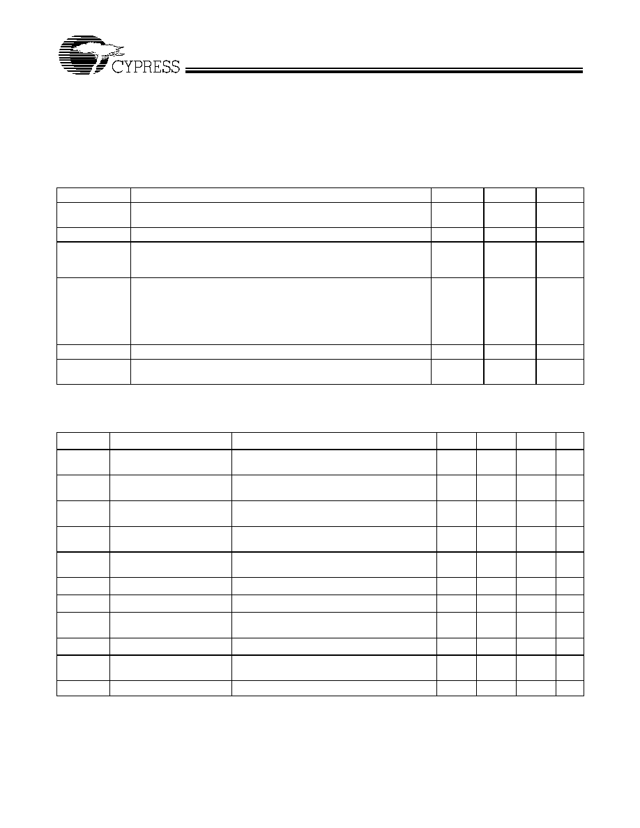
Die Configuration
CY2037 Logic Block Diagram
V
DD
Top View
V
SS
V
DD
X
G
PD/OE
CLKOUT
V
SS
X
G
PD/OE
X
D
CONFIGURATION
CRYSTAL
CLKOUT
/ 1, 2, 4, 8, 16, 32, 64, 128
N/C / Xx
[1]
X
D
N/C
OSCILLATOR
1
2
3
4
5
6
7
8
9
11
or FS
or FS
MUX
HIGH
ACCURACY
PLL
EPROM
N/C
10
7C803xx
Note:
1.
For Customers not bonding X
D
or X
G
pad to external pins, an alternative bonding option would be shorting the Xx pad to the X
D
pad.
CY2037
Document #: 38-07354 Rev. *A
Page 3 of 9
EPROM Configuration Block
Table 1 summarizes the features which are configurable by
EPROM. Please refer to the "7C8038x/7C8034X
Programming Specification" for further details. The specifica-
tion can be obtained from your Cypress factory representative.
PLL Output Frequency
The CY2037 contains a high resolution PLL with 12 bit multi-
plier and 10 bit divider.The output frequency of the PLL is de-
termined by the following formula:
where P is the feedback counter value and Q is the reference
counter value. P and Q are EPROM programmable values.
Power Management features (except CY2037-3)
The CY2037 contains EPROM programmable PWR_DWN
and OE functions. If Powerdown is selected, all active circuitry
on the chip is shut down when the control pin goes low. The
oscillator and PLL circuits must re-lock when the part leaves
Powerdown Mode. If Output Enable mode is selected, the out-
put is tri-stated and weakly pulled low when the Control pin
goes low. In this mode the oscillator and PLL circuits continue
to operate, allowing a rapid return to normal operation when
the Control input is deasserted.
In addition, the PWR_DWN and OE modes can be pro-
grammed to occur synchronously or asynchronously with re-
spect to the output signal. When the asynchronous setting is
used, the powerdown or output disable occurs immediately
(allowing for logic delays) irrespective of position in the clock
cycle. However, when the synchronous setting is used, the
part waits for a falling edge at the output before powerdown or
output enable signal is initiated, thus preventing output glitch-
es. In either asynchronous or synchronous setting, the output
is always enabled synchronously by waiting for the next falling
edge of the output.
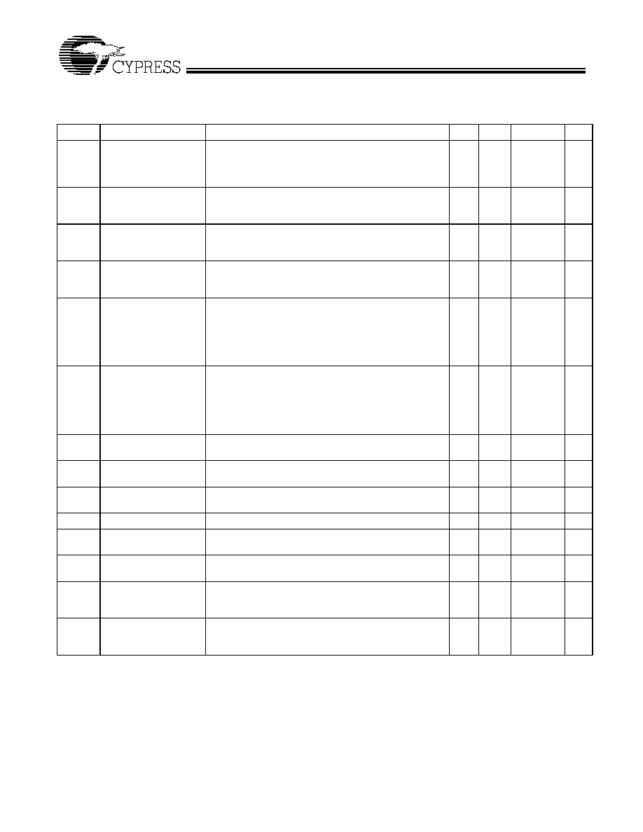
Crystal Oscillator Tuning Circuit
The CY2037 contains a unique tuning circuit to fine-tune the
output frequency of the device. The tuning circuit consists of
an array of eleven load capacitors on both sides of the oscilla-
tor drive inverter. The capacitor load values are EPROM pro-
grammable and can be increased in small increments. As the
capacitor load is increased the circuit is fine-tuned to a lower
frequency. The capacitor load values vary from 0.17 pF to 8 pF
for a 100:1 total control ratio. The tuning increments are shown
in the table below. Please refer to the "7C8038x/7C8034x Pro-
gramming Specification" for further details.
Difference Between CY2037A and CY2037-2
The CY2037A contains a shadow register in addition to the
EPROM register. The shadow register is an exact copy of the
EPROM register and is the default register when the Valid bit
is not set. It is useful when the prototype or production envi-
ronment calls for measuring and adjusting the CLKOUT fre-
quency numerous times. Multiple adjustments can be per-
formed with the shadow register. Once the desired frequency
is achieved the EPROM register is permanently programmed.
Some production flows do not require the use of the shadow
register. If this is the case, then the CY2037-2 is the device of
choice. The CY2037-2 has a disabled shadow register.
The CY2037-3 contains the shadow register.
Frequency Select Feature of CY2037-3
The CY2037-3 contains a frequency select function in place of
the powerdown and the output enable functions. With the
frequency select feature, customers can switch two different
frequencies that are configured in the two EPROM rows The
definition of the Frequency select pin (FS) is shown in the fol-
lowing table.
Table 1. EPROM Adjustable Features
Adjust
Frequency
Feedback counter value (P)
Reference counter value (Q)
Output divider selection
Oscillator Tuning (load capacitance values)
Duty cycle levels (TTL or CMOS)
Power management mode (OE or PWR_DWN)
Power management timing
(synchronous or asynchronous)
F
PLL
2
P
5
+
(
)
·
Q
2
+
(
)
---------------------------
F
REF
·
=
Die Pad Summary
Name
Die Pad
Description
V
DD
1,2
Voltage supply
V
SS
8,9
Ground
X
D
4
Crystal connection.
X
X
3
No Connect. (For customers not bonding X
D
or X
G
pad to external pins, an alternative bonding option
would be shorting this pad to XD pad.)
X
G
6
Crystal connection.
PD/OE or FS
7
CY2037A and CY2037-2--EPROM programmable power down or output enable pad.
CY2037-3--Frequency Select.
Serves as V
PP
in programming mode for all devices
CLKOUT
11
Clock output. Also serves as three-state input during programming.
N/C
5,10
No Connect. (Do not bond to these pads)
CY2037
Document #: 38-07354 Rev. *A
Page 4 of 9
Crystal Oscillator Tuning Circuit
Device Functionality: Output Frequencies
Parameter
Description
Condition
Min.
Max.
Unit
Fo
Output frequency
V
DD
= 4.5V5.5V
1
133
MHz
V
DD
= 3.0V3.6V
1
100
MHz
V
DD
= 2.7V3.0V
1
66
MHz
Symbol
Description
Min.
Typ.
Max.
Unit
R
f
Feedback resistor, V
DD
= 4.55.5V
Feedback resistor, V
DD
= 2.73.6V
0.5
1.0
2
4
3.5
9.0
M
M
Capacitors have ± 20% Tolerance
C
g
Gate capacitor
13
pF
C
d
Drain Capacitor
9
pF
C
0
Series Cap
0.27
pF
C
1
Series Cap
0.52
pF
C
2
Series Cap
1.00
pF
C
3
Series Cap
0.7
pF
C
4
Series Cap
1.4
pF
C
5
Series Cap
2.6
pF
C
6
Series Cap
5.0
pF
C
7
Series Cap
0.45
pF
C
8
Series Cap
0.85
pF
C
9
Series Cap
1.7
pF
C
10
Series Cap
3.3
pF
Table 2. Frequency Select Pin Decoding for CY2037-3
FS Pin
Output Frequency
0
From EPROM Row 0 Configuration
1
From EPROM Row 1 Configuration
CD = EPROM BIT
T = TRANSISTOR
C = LOAD CAPACITOR
CD6
C6
CD5
C5
CD4
C4
CD3
C3
CD2
C2
CD1
C1
CD0
C0
CD3
C7
CD4
C8
CD5
C9
CD6
C10
External Crystal
Cgo Cdo
Rf
CY2037
Document #: 38-07354 Rev. *A
Page 5 of 9
Absolute Maximum Ratings
(Above which the useful life may be impaired. For user guide-
lines, not tested.)
Supply Voltage ..................................................0.5 to +7.0V
Input Voltage ..............................................0.5V to V
DD
+0.5
Storage Temperature (Non-Condensing) ... 55
°
C to +150
°
C
Junction Temperature ................................. 40
°
C to +100
°
C
Static Discharge Voltage............................................ >2000V
(per MIL-STD-883, Method 3015)
Operating Conditions
Parameter
Description
Min.
Max.
Unit
V
DD
Supply Voltage (3.3V)
Supply Voltage (5.0V)
2.7
4.5
3.6
5.5
V
V
T
AJ
[2]
Operating Temperature, Junction
40
+100
°
C
C
TTL
Max. Capacitive Load on outputs for TTL levels
V
DD
= 4.55.5V, Output frequency = 140 MHz
V
DD
= 4.55.5V, Output frequency = 40133 MHz
50
25
pF
pF
C
CMOS
Max. Capacitive Load on outputs for CMOS levels
V
DD
= 4.55.5V, Output frequency = 166.6MHz
V
DD
= 4.55.5V, Output frequency = 66.6133MHz
V
DD
= 3.03.6V, Output frequency = 140 MHz
V
DD
= 3.03.6V, Output frequency = 40100 MHz
V
DD
= 2.73.0V, Output frequency = 166 MHz
50
25
30
15
15
pF
pF
pF
pF
pF
X
REF
Reference Frequency, input crystal. Fundamental tuned crystals only.
10
30
MHz
t
PU
Power-up time for all VDD's to reach minimum specified voltage (power
ramps must be monotonic)
0.05
50
ms
Electrical Characteristics
Over the Operating Range (Part was characterized in a 20 pin SOIC package with external
crystal, Electrical Characteristics may change with other package types.)
Parameter Description
Test Conditions
Min.
Typ.
Max.
Unit
V
IL
Low-level Input Voltage
V
DD
= 4.5V5.5V
V
DD
= 2.7V3.6V
0.8
0.2V
DD
V
V
V
IH
High-level Input Voltage
V
DD
= 4.5V5.5V
V
DD
= 2.7V3.6V
2.0
0.7V
DD
V
V
V
OL
Low-level Output Voltage
V
DD
= 4.5V5.5V, I
OL
= 16 mA
V
DD
= 2.7V3.6V, I
OL
= 8 mA
0.4
0.4
V
V
V
OHCMOS
High-level Output Voltage,
CMOS levels
V
DD
= 4.5V5.5V, I
OH
= 16 mA
V
DD
= 2.7V3.6V, I
OH
= 8 mA
V
DD
0.4
V
DD
0.4
V
V
V
OHTTL
High-level Output Voltage,
TTL levels
V
DD
= 4.5V5.5V, I
OH
= 8 mA
2.4
V
I
IL
Input Low Current
V
IN
= 0V
10
µ
A
I
IH
Input High Current
V
IN
= V
DD
5
µ
A
I
DD
Power Supply Current,
Unloaded
V
DD
= 4.5V5.5V, Output frequency <= 133MHz
V
DD
= 2.7V3.6V, Output frequency <= 100 MHz
45
25
mA
mA
I
DDS
[3]
Stand-by current
V
DD
= 2.7V3.6V
10
50
µ
A
R
UP
Input Pull-Up Resistor
V
DD
= 4.5V5.5V, V
IN
= 0V
V
DD
= 4.5V5.5V, V
IN
= 0.7V
DD
1.1
50
3.0
100
8.0
200
M
k
I
OE_CLKOUT
CLKOUT Pulldown current
V
DD
= 5.0
20
µ
A
Notes:
2.
This product is sold in die form so operating conditions are specified for the die, or junction temperature
3.
If external reference is used, it is required to stop the reference (set reference to LOW) during power down.
CY2037
Document #: 38-07354 Rev. *A
Page 6 of 9
Output Clock Switching Characteristics
Over the Operating Range
[5]
Symbol
Description
Test Conditions
Min
Typ
Max
Unit
t
1w
Output Duty Cycle at
1.4V, V
DD
= 4.55.5V
t
1w
= t
1A
÷
t
1B
140 MHz, C
L
<= 50 pF
4066 MHz, C
L
<= 15 pF
66125 MHz, C
L
<= 25 pF
125133 MHz, C
L
<= 15 pF
45
45
40
40
55
55
60
60
%
%
%
%
t
1x
Output Duty Cycle at
V
DD
/2, V
DD
= 4.55.5V
t
1x
= t
1A
÷
t
1B
166.6 MHz, C
L
<= 25 pF
66.6125 MHz, C
L
<= 25 pF
125133 MHz, C
L
<= 15 pF
45
40
40
55
60
60
%
%
%
t
1y
Output Duty Cycle at
V
DD
/2, V
DD
= 3.03.6
t
1y
= t
1A
÷
t
1B
140 MHz, C
L
<= 30 pF
40100 MHz, C
L
<= 15 pF
45
40
55
60
%
%
t
1z
Output Duty Cycle at
V
DD
/2, V
DD
= 2.73.0
t
1y
= t
1A
÷
t
1B
140 MHz, C
L
<= 15 pF
4066.6 MHz, C
L
<= 10 pF
40
40
60
60
%
%
t
2
Output Clock Rise time
Between 0.8V2.0V, V
DD
= 4.5V5.5V, C
L
= 50 pF
Between 0.8V2.0V, V
DD
= 4.5V5.5V, C
L
= 25 pF
Between 0.8V2.0V, V
DD
= 4.5V5.5V, C
L
= 15 pF
Between 0.2V
DD
0.8V
DD
, V
DD
= 4.5V5.5V, C
L
= 50 pF
Between 0.2V
DD
0.8V
DD
, V
DD
= 3.0V3.6V, C
L
= 30 pF
Between 0.2V
DD
0.8V
DD
, V
DD
= 2.7V3.6V, C
L
= 15 pF
1.8
1.2
0.9
3.4
4.0
2.4
ns
ns
ns
ns
ns
ns
t
3
Output Clock Fall time
Between 0.8V2.0V, V
DD
= 4.5V5.5V, C
L
= 50 pF
Between 0.8V2.0V, V
DD
= 4.5V5.5V, C
L
= 25 pF
Between 0.8V2.0V, V
DD
= 4.5V5.5V, C
L
= 15 pF
Between 0.2V
DD
0.8V
DD
, V
DD
= 4.5V-5.5V, C
L
= 50 pF
Between 0.2V
DD
0.8V
DD
, V
DD
= 3.0V3.6V, C
L
= 30 pF
Between 0.2V
DD
0.8V
DD
, V
DD
= 2.7V3.6V, C
L
= 15 pF
1.8
1.2
0.9
3.4
4.0
2.4
ns
ns
ns
ns
ns
ns
t
4
Start-up time out of
power-down
PWR_DWN pin LOW to HIGH
[4]
1
2
ms
t
5a
Power Down delay time
(synchronous setting)
PWR_DWN pin LOW to output LOW
(T = period of Output clk)
T/2
T+10
ns
t
5b
Power Down delay time
(asynchronous setting)
PWR_DWN pin LOW to output LOW
10
15
ns
t
6
Power Up time
From power on
[4]
1
2
ms
t
7a
Output disable time
(synchronous setting)
OE pin LOW to output Hi-Z
(T = period of output clk)
T/2
T+10
ns
t
7b
Output disable time
(asynchronous setting)
OE pin LOW to output Hi-Z
10
15
ns
t
8
Output enable time
(always synchronous
enable)
OE pin LOW to HIGH
(T = period of output clk)
T
1.5T+25
ns
t
9
Peak-to-Peak Period
Jitter
V
DD
= 4.5V5.5V, Fo > 33 MHz, VCO > 100 MHz
V
DD
= 2.7V3.6V, Fo > 33 MHz, VCO > 100 MHz
V
DD
= 2.7V5.5V, Fo < 33 MHz
±100
±125
±250
±125
±200
1% of F
O
ps
ps
ps
Notes:
4.
Oscillator start time cannot be guaranteed for all crystal types. This specification is for operation with AT cut crystals with ESR < 70 ohms.
5.
Not all parameters measured in production testing.
CY2037
Document #: 38-07354 Rev. *A
Page 7 of 9
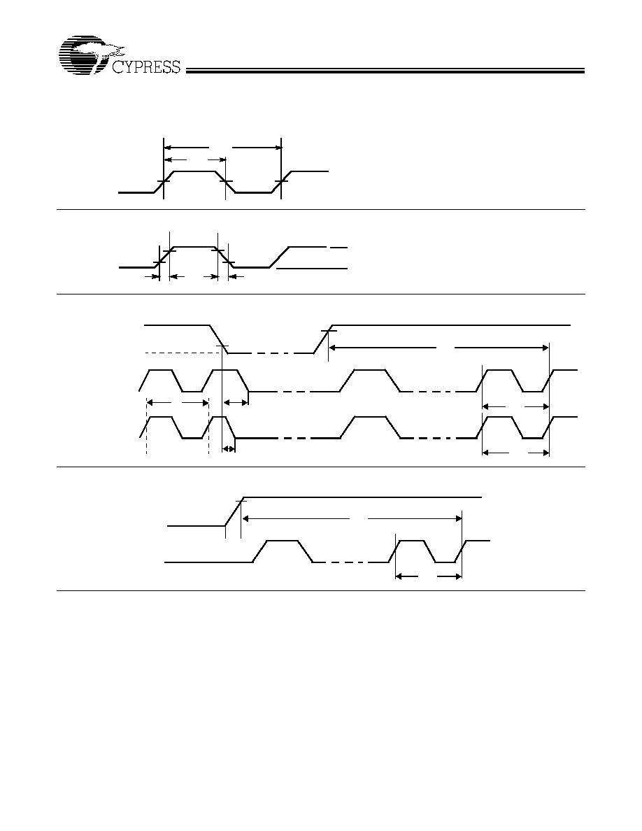
Switching Waveforms
Notes:
6.
In synchronous mode the powerdown or output three-state is not initiated until the next falling edge of the output clock.
7.
In asynchronous mode the powerdown or output three-state occurs within 25n s irrespective of position in the ouput clock cycle.
Duty Cycle Timing (t
1w,
t
1x,
t
1y
, t
1z
)
t
1A
t
1B
OUTPUT
Output Rise/Fall Time
OUTPUT
t
2
V
DD
0V
t
3
Power Down Timing (synchronous and asynchronous modes)
CLKOUT
V
DD
t
4
1/f
t
5a
V
IL
V
IH
POWER
DOWN
0V
1/f
t
5b
CLKOUT
T
(synchronous
[6
]
)
(asynchronous
[7
]
)
Power Up Timing
CLKOUT
V
DD
t
6
1/f
V
DD
10%
POWER
UP
0V
min. 30
µ
s
max. 30 ms
CY2037
Document #: 38-07354 Rev. *A
Page 8 of 9
© Cypress Semiconductor Corporation, 2002. The information contained herein is subject to change without notice. Cypress Semiconductor Corporation assumes no responsibility for the use
of any circuitry other than circuitry embodied in a Cypress Semiconductor product. Nor does it convey or imply any license under patent or other rights. Cypress Semiconductor does not authorize
its products for use as critical components in life-support systems where a malfunction or failure may reasonably be expected to result in significant injury to the user. The inclusion of Cypress
Semiconductor products in life-support systems application implies that the manufacturer assumes all risk of such use and in doing so indemnifies Cypress Semiconductor against all charges.
Ordering Information
[8]
Note:
8.
The only difference between the CY2037A and the CY2037-2 is: The CY2037-2 has the shadow register disabled. The CY2037-3 replaces the power-down
options with a Frequency Select, and contains the shadow register.
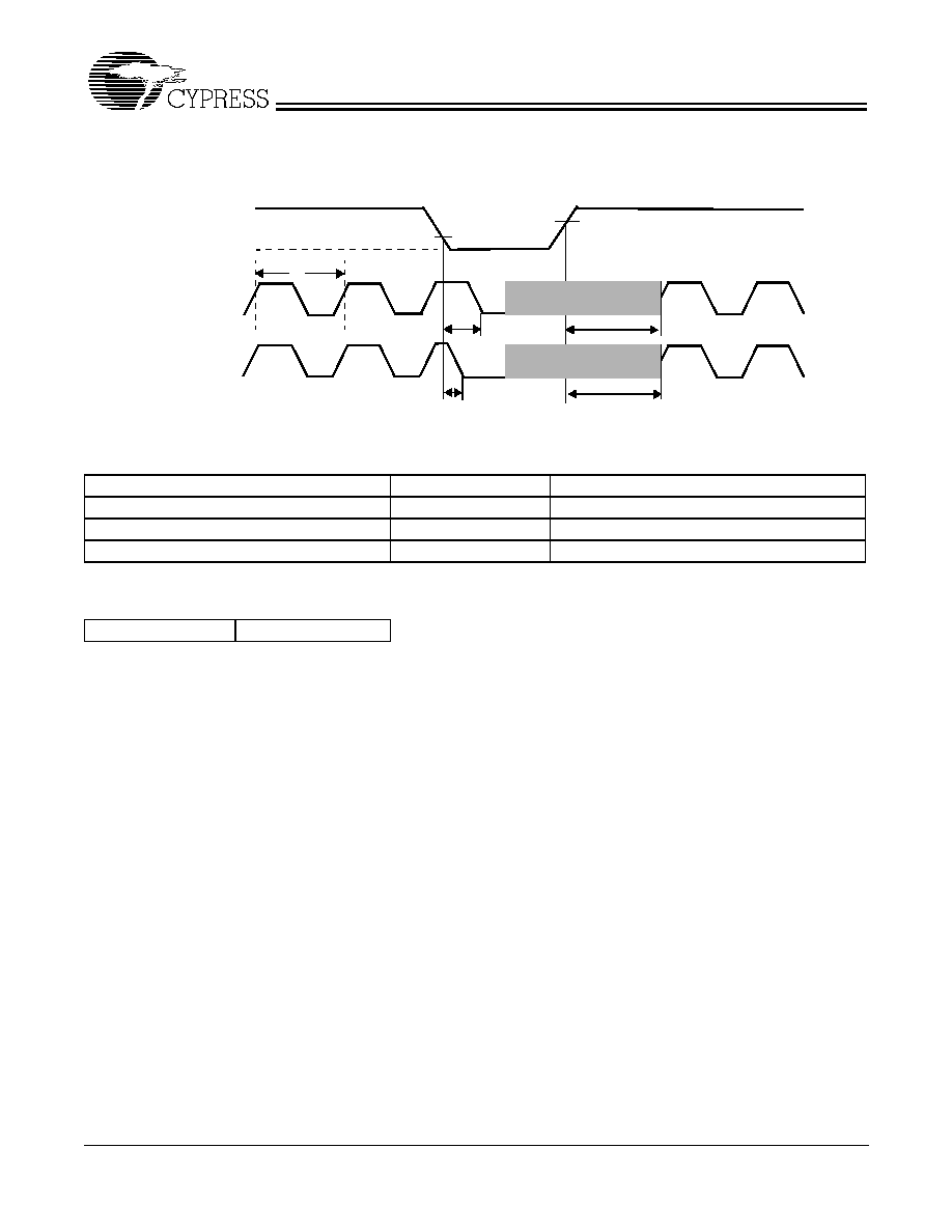
Switching Waveforms
(continued)
CLKOUT
V
DD
OUTPUT
ENABLE
0V
Output Enable Timing (synchronous and asynchronous modes)
V
IL
V
IH
t
7a
t
8
High Impedance
CLKOUT
t
7b
t
8
High Impedance
T
(synchronous
[6
]
)
(asynchronous
[7
]
)
Ordering Code
Type
Operating Range
CY2037AWAF
Wafer
Industrial
CY2037-2WAF
Wafer
Industrial
CY2037-3WAF
Wafer
Industrial
Die Information
Wafer Thickness
14 ±0.5 mils

CY2037
Document #: 38-07354 Rev. *A
Page 9 of 9
Document Title: CY2037 High-Accuracy EPROM Programmable PLL Die for Crystal Oscillators
Document Number: 38-07354
REV.
ECN NO.
Issue
Date
Orig. of
Change
Description of Change
**
112248
03/01/02
DSG
Change from Spec number: 38-00679 to 38-07354
*A
121857
12/14/02
RBI
Power up requirements added to Operating Conditions Information