
133-MHz Spread Spectrum Clock Synthesizer/Driver
with AGP, USB, and DRCG Support
CY2210
Cypress Semiconductor Corporation
∑
3901 North First Street
∑
San Jose
∑
CA 95134
∑
408-943-2600
Document #: 38-07204 Rev. *A
Revised December 14, 2002
0
Features
Benefits
∑ Mixed 2.5V and 3.3V Operation
∑ Compliant to Intel
Æ
CK133 (CY2210-3) & CK133W
(CY2210-2) synthesizer and driver specification
Usable with Pentium
Æ
II and Pentium
Æ
III processors
∑ Multiple output clocks at different frequencies
-- Four CPU clocks, up to 133 MHz
-- Eight synchronous PCI clocks, 1 free-running
-- Two CPU/2 clocks, at one-half the CPU frequency
-- Four AGP clocks at 66 MHz
-- Three synchronous APIC clocks, at 16.67 MHz
-- One USB clock at 48 MHz
-- Two reference clocks at 14.318 MHz
Single-chip main motherboard clock generator
-- Driven together, support 4 CPUs and a chipset
-- Support for 4 PCI slots and chipset
-- Drives up to two main memory clock generators, includ-
ing DRCG (CPUCLK/2)
-- Support for multiple AGP slots
-- Support multiprocessing systems
-- Supports USB frequencies and I/O chip
∑ Spread Spectrum clocking
-- 32.5-kHz modulation frequency @ 133 MHz
-- 33.1-kHz modulation frequency @ 100 MHz for
CY2210-02/03
-- 33.4-kHz modulation frequency @ 100 MHz for
CY2210-04
-- EPROM programmable percentage of spreading.
Default is ≠0.6%, which is recommended by Intel
Enables reduction of EMI in some systems
∑ Power-down features
Supports mobile systems
∑ Three Select inputs
Supports up to eight CPU clock frequencies
∑ Low-skew and low-jitter outputs
Meets tight system timing requirements at high frequency
∑ OE and Test Mode support
Enables ATE and "bed of nails" testing
∑ 56-pin SSOP package
Widely available, standard package enables lower cost
Intel and Pentium are registered trademarks of Intel Corporation.
Logic Block Diagram
EPROM
XTALOUT
XTALIN
APICCLK [0≠2] (16.67 MHz)
14.318
MHz
OSC.
PCICLK_F (33.33 MHz)
SEL1
CPU
PLL
REFCLK [0≠1] (14.318 MHz)
CPUCLK [0≠3]
PCICLK [1≠7] (33.33 MHz)
SYS
PLL
USBCLK (48 MHz)
CPU_STOP
PCI_STOP
SEL0
SEL133
CPUCLK/2 [0≠1] (DRCG)
Divider,
EPROM-
ProgDelay
and
Stop Logic
PWR_DWN
AGPCLK [0≠3] (66.67 MHz)
SPREAD
SSOP
Top View
1
2
3
4
5
6
7
8
9
10
11
12
33
32
31
30
29
36
35
V
SSREF
34
13
14
15
16
17
18
19
20
21
22
23
24
45
44
43
42
41
37
38
39
40
48
47
46
REFCLK0
REFCLK1
V
DDREF
25
26
27
28
49
52
51
50
53
56
55
54
V
DDPCI
PCICLK6
V
DDAGP
V
DDUSB
SPREAD
V
SSCPU
V
DDCPU
APICCLK0
V
SSPCI
PCICLK5
V
SSAGP
AGPCLK3
PCI_STOP
V
DDCPU
CPUCLK/2
V
DDAPIC
XTALIN
XTALOUT
PCICLK_F
PCICLK1
PCICLK2
PCICLK3
V
SSPCI
PCICLK4
V
DDPCI
PCICLK7
V
SSPCI
AGPCLK0
AGPCLK1
V
SSAGP
AGPCLK2
SEL1
SEL0
PWR_DWN
CPU_STOP
AV
SS
AV
DD
CPUCLK0
CPUCLK1
V
SSCPU
CPUCLK2
CPUCLK3
V
SSCPU/2
CPUCLK/2
V
DDCPU/2
V
SSAPIC
APICCLK1
APICCLK2
V
DDAGP
SEL133
USBCLK
V
SSUSB
C
Y
22
10
-2
/
-
3/
-4
(DRCG)
(DRCG)
Pin Configuration

CY2210
Document #: 38-07204 Rev. *A
Page 2 of 10
Pin Summary
Name
Pins
Description
V
SSREF
1
3.3V Reference ground
V
DDREF
4
3.3V Reference voltage supply
V
SSPCI
7, 13, 19
3.3V PCI ground
V
DDPCI
10, 16
3.3V PCI voltage supply
V
SSAGP
20, 24
3.3V AGP ground
V
DDAGP
23, 27
3.3V AGP voltage supply
V
SSUSB
29
3.3V USB ground
V
DDUSB
31
3.3V USB voltage supply
V
SSCPU
40, 44
2.5V CPU ground
V
DDCPU
43, 47
2.5V CPU voltage supply
V
SSCPU
/2
48
2.5V CPU/2 ground
V
DDCPU
/2
51
2.5V CPU/2 voltage supply
V
SSAPIC
52
2.5V APIC ground
V
DDAPIC
56
2.5V APIC voltage supply
AV
SS
38
Analog ground to PLL and Core
AV
DD
39
Analog voltage supply to PLL and Core
XTALIN
[1]
5
Reference crystal input
XTALOUT
[1]
6
Reference crystal feedback
CPUCLK [0≠3]
41, 42, 45, 46
CPU clock outputs
PCICLK [1≠7]
9, 11, 12, 14, 15, 17, 18
PCI clock outputs, synchronously running at 33.33 MHz
PCICLK_F
8
Free running PCI clock
CPUCLK/2
49, 50
CPU/2 clock outputs, drive memory clock generator
AGPCLK [0≠3]
21, 22, 25, 26
AGP clock outputs, running at 66.66 MHz
APICCLK [0≠2]
53, 54, 55
APIC clock outputs, running at 16.67 MHz
REFCLK [0≠1]
2, 3
Reference clock outputs, 14.318 MHz
USBCLK
30
48-MHz USB clock output
CPU_STOP
36
Active LOW input, disables CPU and AGP clocks when asserted
PCI_STOP
37
Active LOW input, disables PCI clocks when asserted
PWR_DWN
35
Active LOW input, powers down part when asserted
SPREAD
34
Active LOW input, enables spread spectrum when asserted
SEL1
33
CPU frequency select input (See Function Table)
SEL0
32
CPU frequency select input (See Function Table)
SEL133
28
CPU frequency select input (See Function Table)
Note:
1.
For best accuracy, use a parallel-resonant crystal, C
LOAD
= 18 pF. For crystals with different C
LOAD
, please refer to the application note, "Crystal Oscillator
Topics."

CY2210
Document #: 38-07204 Rev. *A
Page 3 of 10
Notes:
2.
TCLK is a test clock driven in on the XTALIN input in test mode.
3.
Only CY2210-2 supports this option. In CY2210-3, this selection is defined as "N/A" or "Reserved".
Function Table
[2]
SEL133
SEL1
SEL0
CPUCLK
(MHz)
CPUCLK/2
(MHz)
AGPCLK
(MHz)
PCICLK
(MHz)
USBCLK
(MHz)
REFCLK
(MHz)
APICCLK
(MHz)
0
0
0
Hi-Z
Hi-Z
Hi-Z
Hi-Z
Hi-Z
Hi-Z
Hi-Z
0
0
1
100.227
[3]
50.114
[3]
66.818
[3]
33.409
[3]
48.008
[3]
14.318
[3]
16.705
[3]
0
1
0
100
50
66.67
33.33
OFF
14.318
16.67
0
1
1
100
50
66.67
33.33
48
14.318
16.67
1
0
0
TCLK/2
TCLK/4
TCLK/4
TCLK/8
TCLK/2
TCLK
TCLK/16
1
0
1
N/A
N/A
N/A
N/A
N/A
N/A
N/A
1
1
0
133.33
66.67
66.67
33.33
OFF
14.318
16.67
1
1
1
133.33
66.67
66.67
33.33
48
14.318
16.67
Actual Clock Frequency Values
Clock
Output
Target
Frequency
(MHz)
Actual
Frequency
(MHz)
PPM
-2
-3
-4
-2
-3
-4
-2
-3
-4
CPUCLK
100.0
100.0
100.0
99.126
99.126
100.227
≠8740
≠8740
+2714
CPUCLK
133.33
133.33
133.33
132.769
132.769
132.769
≠4208
≠4208
≠4208
USBCLK
48.0
48.0
48.0
48.008
48.008
48.008
167
167
167
Clock Enable Configuration
CPU_STOP
PWR_DWN
PCI_STOP
CPUCLK
CPUCLK/2
AGP
PCI
PCI_F
REF
APIC
OSC.
VCOs
X
0
X
LOW
LOW
LOW
LOW
LOW
LOW
OFF
OFF
0
1
0
LOW
ON
LOW
LOW
ON
ON
ON
ON
0
1
1
LOW
ON
LOW
ON
ON
ON
ON
ON
1
1
0
ON
ON
ON
LOW
ON
ON
ON
ON
1
1
1
ON
ON
ON
ON
ON
ON
ON
ON
Clock Driver Impedances
Impedance
Buffer Name
V
DD
Range
Buffer Type
Minimum
Typical
Maximum
CPU, CPU/2, APIC
2.375≠2.625
Type 1
13.5
29
45
USB, REF
3.135≠3.465
Type 3
20
40
60
PCI, AGP
3.135≠3.465
Type 5
12
30
55

CY2210
Document #: 38-07204 Rev. *A
Page 4 of 10
Maximum Ratings
(Above which the useful life may be impaired. For user guide-
lines, not tested.)
Supply Voltage ..................................................≠0.5 to +7.0V
Input Voltage .............................................. ≠0.5V to V
DD
+0.5
Storage Temperature (Non-Condensing) ... ≠65
∞
C to +150
∞
C
Junction Temperature ............................................... +150
∞
C
Package Power Dissipation.............................................. 1W
Static Discharge Voltage
(per MIL-STD-883, Method 3015) ............................. >2000V
Operating Conditions
Over which Electrical Parameters are Guaranteed
Parameter
Description
Min.
Max.
Unit
V
DDREF
, V
DDPCI
, AV
DD
,
V
DDAGP
,
V
DDUSB
3.3V Supply Voltages
3.135
3.465
V
V
DDCPU
, V
DDCPU/2
CPU and CPU/2 Supply Voltage
2.375
2.625
V
V
DDAPIC
APIC Supply Voltage
2.375
2.625
V
T
A
Operating Temperature, Ambient
0
70
∞
C
C
L
Max. Capacitive Load on
CPUCLK, CPUCLK/2, USBCLK, REF, APIC
PCICLK, AGP
20
30
pF
f
(REF)
Reference Frequency, Oscillator Nominal Value
14.318
14.318
MHz
t
PU
Power-up time for all VDD's to reach minimum
specified voltage (power ramps must be monotonic)
0.05
50
ms
Electrical Characteristics
Over the Operating Range
Parameter
Description
Test Conditions
Min. Max. Unit
V
IH
High-level Input Voltage
Except Crystal Pads. Threshold voltage for crystal pads = V
DD
/2
2.0
V
V
IL
Low-level Input Voltage
Except Crystal Pads
0.8
V
V
OH
High-level Output Voltage
[4]
CPU, CPU/2, APIC
I
OH
= ≠1 mA
2.0
V
USB, REF, PCI, AGP
I
OH
= ≠1 mA
2.4
V
OL
Low-level Output Voltage
[4]
CPU, CPU/2, APIC
I
OL
= 1 mA
0.4
V
USB, REF, PCI, AGP
I
OL
= 1 mA
0.4
I
IH
Input High Current
0 < V
IN
< V
DD
10
µ
A
I
IL
Input Low Current
0 < V
IN
< V
DD
10
µ
A
I
OH
High-level Output Cur-
rent
[4]
CPU, CPU/2
V
OH
= 2.0V
≠16
≠60
mA
APIC
V
OH
= 2.0V
≠20
≠72
USB, REF
V
OH
= 2.4V
≠15
≠51
AGP, PCI
V
OH
= 2.4V
≠30 ≠100
I
OL
Low-level Output Current
[4]
CPU, CPU/2
V
OL
= 0.4V
19
49
mA
APIC
V
OL
= 0.4V
25
58
USB, REF
V
OL
= 0.4V
10
24
AGP, PCI
V
OL
= 0.4V
20
49
I
OZ
Output Leakage Current
Three-state
10
µ
A
I
DD2
2.5V Power Supply Current AV
DD
/V
DD33
= 3.465V, V
DD25
= 2.625V, F
CPU
= 133 MHz
90
mA
I
DD3
3.3V Power Supply Current AV
DD
/V
DD33
= 3.465V, V
DD25
= 2.625V, F
CPU
= 133 MHz
160
mA
I
DDPD2
2.5V Shutdown Current
AV
DD
/V
DD33
= 3.465V, V
DD25
= 2.625V
100
µ
A
I
DDPD3
3.3V Shutdown Current
AV
DD
/V
DDQ3
= 3.465V, V
DD25
= 2.625V
200
µ
A
Note:
4.
Parameter is guaranteed by design and characterization. Not 100% tested in production.

CY2210
Document #: 38-07204 Rev. *A
Page 5 of 10
Switching Characteristics
[4, 5]
Over the Operating Range
Parameter
Output
Description
Test Conditions
Min.
Max.
Unit
t
1
All
Output Duty Cycle
[6]
t
1A
/t
1B
45
55
%
t
2
CPU, CPU/2,
APIC
Rising Edge Rate
Between 0.4V and 2.0V
1.0
4.0
V/ns
t
2
USB, REF
Rising Edge Rate
Between 0.4V and 2.4V
0.5
2.0
V/ns
t
2
PCI, AGP
Rising Edge Rate
Between 0.4V and 2.4V
1.0
4.0
V/ns
t
3
CPU, CPU/2,
APIC
Falling Edge Rate
Between 2.0V and 0.4V
1.0
4.0
V/ns
t
3
USB, REF
Falling Edge Rate
Between 2.4V and 0.4V
0.5
2.0
V/ns
t
3
PCI, AGP
Falling Edge Rate
Between 2.4V and 0.4V
1.0
4.0
V/ns
t
6
CPU
CPU-CPU Skew
Measured at 1.25V
175
ps
t
7
CPU/2
CPU/2-CPU/2 Skew
Measured at 1.25V
175
ps
t
8
APIC
APIC-APIC Skew
Measured at 1.25V
250
ps
t
9
AGP
AGP-AGP Skew
Measured at 1.5V
250
ps
t
10
PCI
PCI-PCI Skew
Measured at 1.5V
500
ps
t
11
CPU, AGP
CPU-AGP Clock Skew
CPU leads. Measured at 1.25V for
2.5V clocks and 1.5V for 3.3V clocks
0
1.5
ns
t
12
AGP, PCI
AGP-PCI Clock Skew
AGP leads. Measured at 1.5V
1.5
4.0
ns
t
13
CPU, APIC
CPU-APIC Clock Skew
CPU leads. Measured at 1.25V
1.5
4
ns
t
14
CPU, PCI
CPU-PCI Clock Skew
CPU leads. Measured at 1.25V clocks
and 1.5V for 3.3V clocks
1.5
4
ns
CPU
Cycle-Cycle Clock Jitter
With all outputs running (CY2210-2)
150
ps
CPU
Cycle-Cycle Clock Jitter
With all outputs running
(CY2210-3/-4)
250
ps
CPU
Cycle-Cycle Clock Jitter
With the USB output turned off
(CY2210-3/-4)
200
ps
CPU/2
Cycle-Cycle Clock Jitter
250
ps
APIC
Cycle-Cycle Clock Jitter
500
ps
USB
Cycle-Cycle Clock Jitter
500
ps
AGP
Cycle-Cycle Clock Jitter
500
ps
REF
Cycle-Cycle Clock Jitter
1000
ps
CPU, PCI
Settle Time
CPU and PCI clock stabilization from
power-up
3
ms
Notes:
5.
All parameters specified with loaded outputs.
6.
Duty cycle is measured at 1.5V when V
DD
= 3.3V. When V
DD
= 2.5V, duty cycle is measured at 1.25V.
CY2210
Document #: 38-07204 Rev. *A
Page 6 of 10
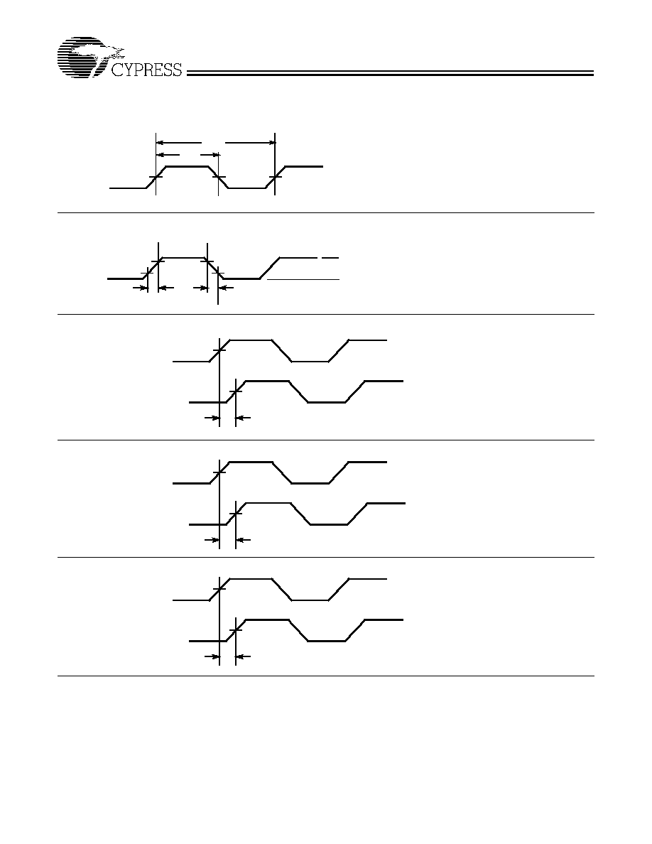
Switching Waveforms
Duty Cycle Timing
t
1A
t
1B
All Outputs Rise/Fall Time
OUTPUT
t
2
V
DD
0V
t
3
CPU-CPU Clock Skew
t
6
CPUCLK
CPUCLK
CPU/2 - CPU/2 Clock Skew
t
7
CPU/2
CPU/2
APIC-APIC Clock Skew
t
8
APIC
APIC

CY2210
Document #: 38-07204 Rev. *A
Page 7 of 10
Switching Waveforms
(continued)
AGP-AGP Clock Skew
t
9
AGP
AGP
PCI-PCI Clock Skew
t
10
PCI
PCI
CPU-AGP Clock Skew
t
11
CPU
AGP
AGP - PCI Clock Skew
t
12
AGP
PCI
CPU-APIC Clock Skew
CPU
t
13
APIC

CY2210
Document #: 38-07204 Rev. *A
Page 8 of 10
Notes:
7.
CPUCLK on and CPUCLK off latency is 2 or 3 CPUCLK cycles.
8.
CPU_STOP may be applied asynchronously. It is synchronized internally.
Switching Waveforms
(continued)
CPU-PCI Clock Skew
CPU
t
14
PCI
CPU_STOP Timing
CPUCLK
(Internal)
PCICLK
(Internal)
PCICLK
(Free-Running)
CPU_STOP
CPU, CPU/2, AGP
(External)
[7, 8]
PCI_STOP
CPUCLK
(Internal)
PCICLK
(Internal)
PCICLK
PCI_STOP
PCICLK
(External)
(Free-Running)
PWR_DOWN
CPUCLK
(Internal)
PCICLK
(Internal)
PWR_DWN
PCICLK
CPUCLK
(External)
(External)
VCO
Crystal
Shaded section on the VCO and Crystal waveforms indicates that the VCO and crystal oscillator are active, and there is a valid clock.

CY2210
Document #: 38-07204 Rev. *A
Page 9 of 10
© Cypress Semiconductor Corporation, 2001. The information contained herein is subject to change without notice. Cypress Semiconductor Corporation assumes no responsibility for the use
of any circuitry other than circuitry embodied in a Cypress Semiconductor product. Nor does it convey or imply any license under patent or other rights. Cypress Semiconductor does not authorize
its products for use as critical components in life-support systems where a malfunction or failure may reasonably be expected to result in significant injury to the user. The inclusion of Cypress
Semiconductor products in life-support systems application implies that the manufacturer assumes all risk of such use and in doing so indemnifies Cypress Semiconductor against all charges.
Test Circuit
Note: All capacitors must be placed as close to the pins as is physically possible.
1, 7, 13, 19, 20, 24, 29, 38, 40, 44, 48, 52
4, 10, 16, 23, 27, 31
V
DDPCI
, V
DDAGP
,
C
LOAD
OUTPUTS
V
DDCPU
, V
DDCPU/2
,
CY2210
43, 47, 51, 56
Note: Each supply pin must have an individual decoupling capacitor.
V
DDUSB
, V
DDREF
,
V
DDAPIC
AV
DD
Ordering Information
Ordering Code
Package
Name
Package Type
Operating
Range
CY2210PVC-2/-3/-4
O56
56-Pin SSOP
Commercial
Package Diagram
56-Lead Shrunk Small Outline Package O56
51-85062-*C

CY2210
Document #: 38-07204 Rev. *A
Page 10 of 10
Document Title: CY2210 133-MHz Spread Spectrum Clock Synthesizer/Driver with AGP, USB, and DRCG Support
Document Number: 38-07204
REV.
ECN NO.
Issue
Date
Orig. of
Change
Description of Change
**
111724
01/10/02
DSG
Change from Spec number: 38-00888 to 38-07204
*A
121839
12/14/02
RBI
Power up requirements added to Operating Conditions Information