
High-Frequency Programmable PECL
Clock Generator
CY2213
Cypress Semiconductor Corporation
∑
3901 North First Street
∑
San Jose
,
CA 95134
∑
408-943-2600
Document #: 38-07263 Rev. *E
Revised May 23, 2003
1CY2213
Features
Benefits
∑ Jitter peak-peak (TYPICAL) = 35 ps
High-accuracy clock generation
∑ LVPECL output
One pair of differential output drivers
∑ Default Select option
Phase-locked loop (PLL) multiplier select
∑ Serially-configurable multiply ratios
Eight-bit feedback counter and six-bit reference counter for high accuracy
∑ Output edge-rate control
Minimize electromagnetic interference (EMI)
∑ 16-pin TSSOP
Industry-standard, low-cost package saves on board space
∑ High frequency
125- to 400-MHz (-1) or to 500-MHz (-2) extended output range for high-speed
applications
∑ 3.3V operation
Enables application compatibility
Block Diagram
1
2
3
4
5
6
7
8
9
12
11
10
13
16
15
14
CLKB
CLK
SER CLK
XIN
XOUT
PLL
Xtal
Oscillator
xM
CLK
VDD
S
SER DATA
VSS
CLKB
VSS
VDD
XIN
VSS
VDDX
SER CLK
OE
VDD
XOUT
VSSX
SER DATA
S
OE
16-pin TSSOP
Pin Configuration
CY2213

CY2213
Document #: 38-07263 Rev. *E
Page 2 of 10
CY2213 Two-Wire Serial Interface
Introduction
The CY2213 has a two-wire serial interface designed for data
transfer operations, and is used for programming the P and Q
values for frequency generation. S
clk
is the serial clock line
controlled by the master device. S
data
is a serial bidirectional
data line. The CY2213 is a slave device and can either read or
write information on the dataline upon request from the master
device.
Figure 1 shows the basic bus connections between master
and slave device. The buses are shared by a number of
devices and are pulled high by a pull-up resistor.
Serial Interface Specifications
Figure 2 shows the basic transmission specification. To begin
and end a transmission, the master device generates a start
signal (S) and a stop signal (P). Start (S) is defined as
switching the S
data
from HIGH to LOW while the S
clk
is at
HIGH. Similarly, stop (P) is defined as switching the S
data
from
LOW to HIGH while holding the S
clk
HIGH. Between these two
signals, data on S
data
is synchronous with the clock on the S
clk
.
Data is allowed to change only at LOW period of clock, and
must be stable at the HIGH period of clock. To acknowledge,
drive the S
data
LOW before the S
clk
rising edge and hold it
LOW until the S
clk
falling edge.
Serial Interface Format
Each slave carries an address. The data transfer is initiated by
a start signal (S). Each transfer segment is 1 byte in length.
The slave address and the read/write bit are first sent from the
master device after the start signal. The addressed slave
device must acknowledge (Ack) the master device. Depending
on the Read/Write bit, the master device will either write data
into (logic 0) or read data (logic 1) from the slave device. Each
time a byte of data is successfully transferred, the receiving
device must acknowledge. At the end of the transfer, the
master device will generate a stop signal (P).
Serial Interface Transfer Format
Figure 2 shows the serial interface transfer format used with
the CY2213. Two dummy bytes must be transferred before the
first data byte. The CY2213 has only three bytes of latches to
store information, and the third byte of data is reserved. Extra
data will be ignored.
Pin Description
Pin Name
Pin Number
Pin Description
VDDX
1
3.3V Power Supply for Crystal Driver
VSSX
2
Ground for Crystal Driver
XOUT
3
Reference Crystal Feedback
XIN
4
Reference Crystal Input
VDD
5
3.3 V Power Supply (all V
DD
pins must be tied directly on board)
OE
6
Output Enable, 0 = output disable, 1 = output enable (no internal pull-up)
VSS
7
Ground
SER CLK
8
Serial Interface Clock
SER DATA
9
Serial Interface Data
VDD
10
3.3V Power Supply (all V
DD
pins must be tied directly on board)
VSS
11
Ground
CLKB
12
LVPECL Output Clock (complement)
CLK
13
LVPECL Output Clock
VSS
14
Ground
VDD
15
3.3V Power Supply (all V
DD
pins must be tied directly on board)
S
16
PLL Multiplier Select Input, Pull-up Resistor Internal
Frequency Table
S
M (PLL Multiplier)
Example Input Crystal Frequency
CLK,CLKB
0
x16
25 MHz
400 MHz
31.25 MHz
500 MHz
1
x8
15.625 MHz
125 MHz
CY2213
Document #: 38-07263 Rev. *E
Page 3 of 10
To program the CY2213 using the two-wire serial interface, set
the SELPQ bit HIGH. The default setting of this bit is LOW. The
P and Q values are determined by the following formulas:
P
final
= (P
7..0
+ 3) * 2
Q
final
= Q
5..0
+ 2.
If the QCNTBYP bit is set HIGH, then Q
final
defaults to a value
of 1. The default setting of this bit is LOW.
If the SELPQ bit is set LOW, the PLL multipliers will be set
using the values in the Select Function Table.
CyberClocksTM has been developed to generate P and Q
values for stable PLL operation. This software is downloadable
from www.cypress.com.
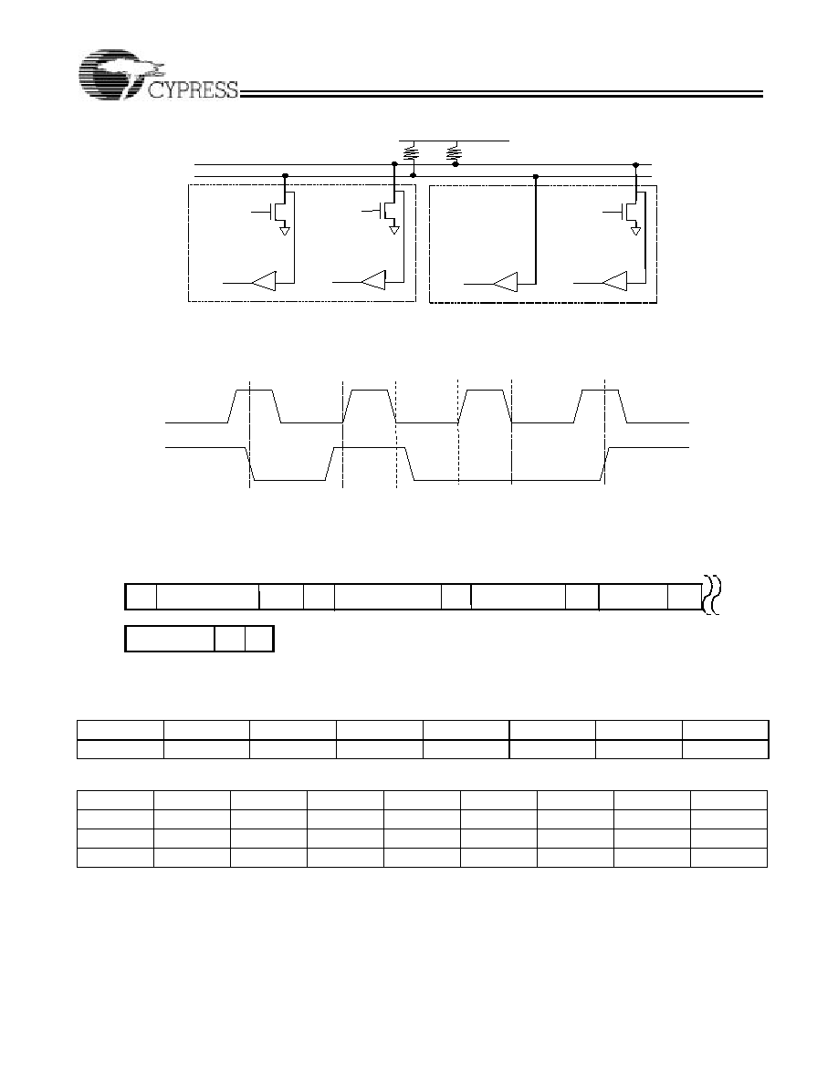
Figure 1. Device Connections
Figure 2. Serial Interface Specifications
Figure 3. CY2213 Transfer Format
Serial Interface Address for the CY2213
A6
A5
A4
A3
A2
A1
A0
R/W
1
1
0
0
1
0
1
0
Serial Interface Programming for the CY2213
b7
b6
b5
b4
b3
b2
b1
b0
Data0
QCNTBYP
SELPQ
Q<5>
Q<4>
Q<3>
Q<2>
Q<1>
Q<0>
Data1
P<7>
P<6>
P<5>
P<4>
P<3>
P<2>
P<1>
P<0>
Data2
Reserved
Reserved
Reserved
Reserved
Reserved
Reserved
Reserved
Reserved
S
c lk
S
d a ta
S
clk
_ C
S
clk
_ in
S
d a ta
_ C
S
d ata
_ in
M a s te r D e vic e
R
p
S
c lk
_ in
S
d ata
_ C
S
d ata
_ in
S lav e D ev ic e
V
D D
R
p
Fig. 2 Serial Interface Specifications
Start (S)
Stop (P)
S
clk
S
data
valid data
Acknowledge
Ack
1 bit
8 bits
Data 1
P
Slave Address
Ack
S
Dummy Byte 0
R/W
Dummy Byte 1
Ack
1 bit
1 bit
Ack
1 bit
7 bits
8 bits
1 bit
Data 0
Ack
1 bit
8 bits
1 bit
8 bits

CY2213
Document #: 38-07263 Rev. *E
Page 4 of 10
PLL Frequency = Reference x P/Q = Output
Absolute Maximum Conditions
The following table reflects stress ratings only, and functional
operation at the maximums are not guaranteed.
Crystal Requirements
Requirements to use parallel mode fundamental xtal. External
capacitors are required in the crystal oscillator circuit. Please
refer to the application note entitled Crystal Oscillator Topics
for details.
DC Electrical Specifications
AC Electrical Specifications
Reference
PLL
Q
P
VCO
Output
Figure 4. PLL Block Diagram
Parameter
Description
Min.
Max.
Unit
V
DD,ABS
Max. voltage on V
DD
, or V
DDX
with respect to ground
≠0.5
4.0
V
V
I, ABS
Max. voltage on any pin with respect to ground
≠0.5
V
DD
+0.5
V
Parameter
Description
Min.
Max.
Unit
X
F
Frequency
10
31.25
MHz
Parameter
Description
Min.
Max.
Unit
V
DD
Supply voltage
3.00
3.60
V
T
A
Ambient operating temperature
0
70
∞C
V
IL
Input signal low voltage at pin S
0.35
V
DD
V
IH
Input signal high voltage at pin S
0.65
V
DD
R
PUP
Internal pull-up resistance
10
100
k
t
PU
Power-up time for all V
DD
s to reach minimum specified voltage
(power ramps must be monotonic)
0.05
500
ms
Parameter
Description
Min.
Max.
Unit
f
IN
Input frequency with driven reference
1
133
MHz
f
XTAL,IN
Input frequency with crystal input
10
31.25
MHz
C
IN,CMOS
Input capacitance at S pin
[1]
10
pF
3.3V DC Device Characteristics (Driving load, Figure 5)
Parameter
Description
Min.
Typ.
Max.
Unit
V
OH
Output high voltage, referenced to V
DD
≠1.02
≠0.95
≠0.88
V
V
OL
Output low voltage, referenced to V
DD
≠1.81
≠1.70
≠1.62
V
3.3V DC Device Characteristics (Driving load, Figure 6)
Parameter
Description
Min.
Typ.
Max.
Unit
V
OH
Output high voltage
1.1
1.2
1.3
V
V
OL
Output low voltage
0
0
0
V
Note:
1.
Capacitance measured at freq. = 1 MHz, DC Bias = 0.9V, and VAC < 100 mV.

CY2213
Document #: 38-07263 Rev. *E
Page 5 of 10
State Transition Characteristics
Specifies the maximum settling time of the CLK and CLKB
outputs from device power-up. For V
DD
and V
DDX
any
sequences are allowed to power-up and power-down the
CY2213.
From
To
Transition Latency
Description
V
DD
/V
DDX
On CLK/CLKB Normal
3 ms
Time from V
DD
/V
DDX
is applied and settled to CLK/CLKB outputs settled.
AC Device Characteristics
Parameter
Description
Min.
Max.
Unit
t
CYCLE
Clock cycle time
2.50 (400 MHz)
8.00 (125 MHz)
ns
t
JCRMS
Cycle-to-cycle RMS jitter
0.25%
% t
CYCLE
At 125-MHz frequency
20
ps
At 400-/500-MHz frequency
6.25/5
ps
t
JCPK
Cycle-to-cycle jitter (pk-pk)
1.75%
% t
CYCLE
At 125-MHz frequency
140
ps
At 200-MHz frequency, XF = 25 MHz
55
ps
At 400-/500-MHz frequency
43.75/35
ps
t
JPRMS
Period jitter RMS
0.25%
% t
CYCLE
At 125-MHz frequency
20
ps
At 400-/500-MHz frequency
6.25/5
ps
t
JPPK
Period jitter (pk-pk)
2.0%
% t
CYCLE
At 125-MHz frequency
160
ps
At 200-MHz frequency, XF = 25 MHz
65
ps
At 400-/500-MHz frequency
50/40
ps
t
JLT
Long term RMS Jitter (P < 20)
1.75%
% t
CYCLE
At 125-MHz frequency
140
ps
At 400-/500-MHz frequency
43.75/35
ps
t
JLT
Long term RMS Jitter (20 < P < 40)
2.5%
% t
CYCLE
At 125-MHz frequency
200
ps
At 400-/500-MHz frequency
62.5/50
ps
t
JLT
Long-term RMS Jitter (40 < P < 60)
3.5%
% t
CYCLE
At 125-MHz frequency
280
ps
At 400-/500-MHz frequency
87.5/70
ps
Phase Noise
Phase Noise at 10 kHz (x8 mode) @ 125 MHz
≠107
≠92
dBc
DC
Long-term average output duty cycle
45
55
%
t
DC,ERR
Cycle-cycle duty cycle error at x8 with
15.625-MHz input
70
ps
t
CR
, t
CF
Output rise and fall times (measured at 20% ≠
80% of V
OHmin
and V
OLmax
)
100
400
ps
BW
LOOP
PLL Loop Bandwidth
50 kHz (≠3 dB)
8 MHz (≠20 dB)