 | –≠–ª–µ–∫—Ç—Ä–æ–Ω–Ω—ã–π –∫–æ–º–ø–æ–Ω–µ–Ω—Ç: CY22313 | –°–∫–∞—á–∞—Ç—å:  PDF PDF  ZIP ZIP |
Two-PLL Clock Generator with
Direct RambusTM (Lite) Support
CY22313
Cypress Semiconductor Corporation
∑
3901 North First Street
∑
San Jose
,
CA 95134
∑
408-943-2600
Document #: 38-07434 Rev. *E
Revised June 29, 2004
Features
∑ Two integrated phase-locked loops (PLLs)
∑ Ultra-accurate PLLs
∑ Direct RambusTM clock support
∑ Two input selects
∑ 3.45V core; 3.45V, 2.5V, 1.8V, and 1.675V outputs
∑ 24-pin TSSOP package
Benefits
∑ High-performance PLL tailored for multimedia applica-
tions
∑ Frequency tolerance within 1 PPM on all frequencies
∑ One pair of differential output drivers, identical speci-
fication to CY2212
∑ Selectable 54.0-/53.946-MHz output and
294.912-/393.216-MHz Rambus
Æ
output
∑ Supports output voltage requirements
∑ Industry-standard packaging saves on board space
Pin Configuration
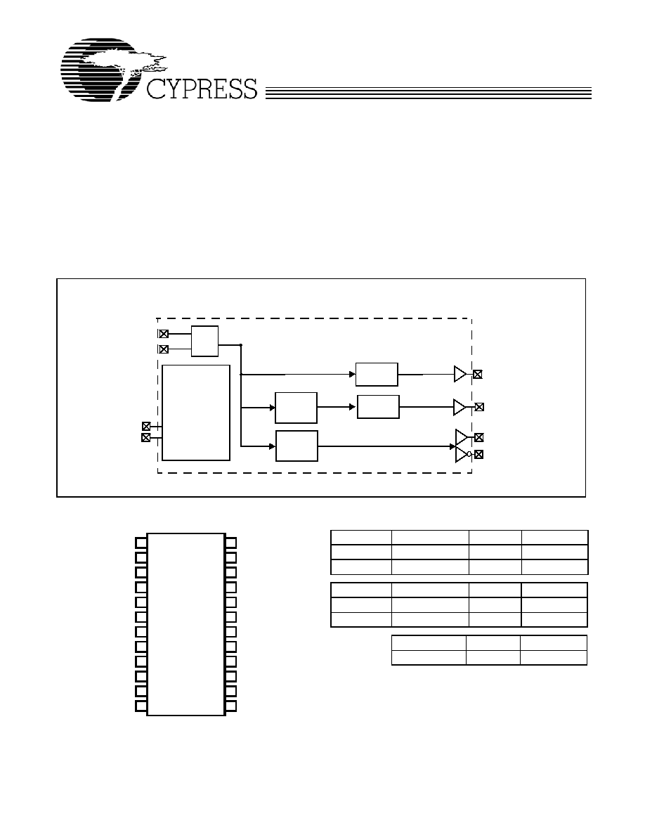
Frequency Select Tables
XIN
XOUT
S
FS
OSC.
PLL1
LCLK
Divider
CLK
54MOUT
Block Diagram
PLL2
CLKB
Divide by 2
XTAL.
CONFIGURATION
LOGIC
VDDRP
1
24
S
VSSRP
2
23
VDDR
Xout
3
22
VSSR
Xin
4
21
CLK
NC
5
20
CLKB
VSSVPA
6
19
VSSR
VDDVPA
7
18
VDDR
VSS54
8
17
NC
54MOUT
9
16
VDDL
FS
10
15
VSSL
VDD54
11
14
LCLK
VDDVP
12
13
VSSVP
FS
54MOUT
Unit
PPM
0
54
MHz
0
1
53.94605395
MHz
≠1
S
CLK, CLKB
Unit
PPM
0
294.912
MHz
0
1
393.216
MHz
0
LCLK
Unit
PPM
9.216
MHz
0

CY22313
Document #: 38-07434 Rev. *E
Page 2 of 9
Pin Definitions
Name
Pin Numbers
Pin Description
V
DDRP
1
Power for DRCG PLL
V
SSRP
2
Ground for DRCG PLL
X
out
3
Crystal Output
X
in
4
Crystal Input
NC
5
Do Not Connect, Leave Floating
V
SSVPA
6
Analog Ground For Video PLL
V
DDVPA
7
Analog Power for Video PLL
V
SS54
8
Ground for 54MOUT
54MOUT
9
54-MHz/53.94605395-MHz Output
FS
10
Frequency Select Pin for 54MOUT (internal pull-down resistor)
V
DD54
11
Power for 54MOUT
V
DDVP
12
Power for Video PLL
V
SSVP
13
Ground for Video PLL
LCLK
14
LCLK Output
V
SSL
15
Ground for LCLK
V
DDL
16
Power for LCLK
NC
17
Do Not Connect, Leave Floating
V
DDR
18
Power for DRCG CLK/CLKB
V
SSR
19
Ground for DRCG CLK/CLKB
CLKB
20
Output Clock to Rambus (complement)
CLK
21
Output Clock to Rambus
V
SSR
22
Ground for DRCG CLK/CLKB
V
DDR
23
Power for DRCG CLK/CLKB
S
24
Frequency Select Pin for DRCG CLK/CLKB (internal pull-up resistor)

CY22313
Document #: 38-07434 Rev. *E
Page 3 of 9
Absolute Maximum Conditions
(Above which the useful life may be impaired. For user guide-
lines; not tested.)
Supply Voltage ............................................... ≠0.5V to +4.0V
DC Input Voltage ..............................≠0.5V to + (V
DD
+ 0.5V)
Storage Temperature.................................. ≠65
∞C to +125∞C
Static Discharge Voltage
(per MIL-STD-883, Method 3015) ............................... 2000V
Latch-up (per JEDEC 17) .................................... > ±200 mA
Recommended Operating Conditions
[1]
Parameter
Description
Min.
Typ
Max.
Unit
V
DDRP
, V
DDVPA,
V
DDVP,
V
DDR
Supply Voltage for PLL's, Crystal Oscillator, and 3.45V Outputs
3.15
3.45
3.6
V
V
DD54
(2.5V)
Supply Voltage for 2.5V Outputs
2.25
2.5
2.75
V
V
DD54
(1.675V)
Supply Voltage for 1.675V Outputs
1.6
1.675
1.75
V
V
DDL
Supply Voltage for 1.8V Outputs
1.6
1.8
2.0
V
t
PU
Power-up time for all V
DDS
to reach minimum specified voltage
(power ramps must be monotonic)
0.05
500
ms
T
A
Operating Temperature, Ambient
0
+85
∞C
C
LOAD_54MOUT
Max. Load Capacitance, CMOS Output
15
pF
f
REF
External Reference Crystal
18.432
MHz
Electrical Specifications
Parameter
Description
Conditions
Min.
Typ.
Max.
Unit
I
OH
[2]
Output High Current, 2.5V outputs
[3]
V
OH
= V
DD
≠ 0.5, V
DD
= 2.5V
8
16
mA
Output High Current, 1.8V outputs
[3]
V
OH
= V
DD
≠ 0.5, V
DD
= 1.8V 6
12
mA
Output High Current, 1.675V outputs
[3]
V
OH
= V
DD
≠ 0.5, V
DD
= 1.675V
5
10
mA
I
OL
[2]
Output Low Current, 2.5V outputs
[3]
V
OL
= 0.5V, V
DD
= 2.5V
8
16
mA
Output Low Current, 1.8V outputs
[3]
V
OL
= 0.5V, V
DD
= 1.8V 6
12
mA
Output Low Current, 1.675V outputs
[3]
V
OL
= 0.5V, V
DD
= 1.675V
5
10
mA
C
XTAL
Crystal Load Capacitance
[3]
Total effective load of internal load caps
11
[4]
pF
C
LOAD_IN
Input Pin Capacitance
[3]
Except crystal pins
7
pF
V
IH
HIGH-Level Input Voltage
CMOS levels,% of V
DDRP
/V
DDVPA
/V
DDVP
70%
V
DD
V
IL
LOW-Level Input Voltage
CMOS levels,% of V
DDRP
/V
DDVPA
/V
DDVP
30%
V
DD
R
I_FS
FS Input Resistor
Pull-down resistor on FS
60
150
225
k
R
I_S
S Input Resistor
Pull-up resistor on S
10
100
k
I
DD
Total Power Supply Current
Sum of all supply currents
125
mA
Direct Rambus Electrical Specifications
[3]
Parameter
Description
Min.
Typ.
Max.
Unit
V
CM
Differential output common-mode voltage
1.35
1.75
V
V
X
Differential output crossing-point voltage
[5]
1.25
1.85
V
V
COS
Output Voltage swing (p-p single-ended)
[6]
0.4
0.7
V
V
COH
Output high voltage
2.1
V
V
COL
Output low voltage
1.0
V
r
OUT
Output dynamic resistance (at pins)
[7]
12
50
Notes:
1.
Unless otherwise noted, Electrical and Switching Characteristics are guaranteed across these operating conditions.
2.
LCLK and 54MOUT outputs only.
3.
Guaranteed by design, not 100% tested.
4.
Identical Crystal Load Capacitance as CY2212ZC-2. Use the same crystal and X
IN
/ X
OUT
board layout as implemented with the original crystal-driven
CY2212ZC-2.
5.
Differential output crossing point voltages shown in Figure 1.
6.
V
COS
= V
OH
≠ V
OL
.
7.
r
OUT
=
V
O
/
I
O
. This is defined at the output pins, not at the measurement point of Figure 9.

CY22313
Document #: 38-07434 Rev. *E
Page 4 of 9
Switching Characteristics
[3]
Parameter
Description
Conditions
Min.
Typ.
Max.
Unit
F
PPM
Frequency Error
Part to Part, does not include PCB variation
[8]
±5
±10
PPM
Over commercial temperature range
[9]
±2
±5
PPM
DC
Output Duty Cycle
Duty cycle for all outputs, measured at V
DD
/2
45
50
55
%
t
3_54, 2.5
54MOUT Rising Edge Slew Rate 20% to 80% of V
DD54
, V
DD54
= 2.5V
0.75
1.2
4.0
V/ns
t
3_54, 1.675
54MOUT Rising Edge Slew Rate 20% to 80% of V
DD54
, V
DD54
= 1.675V
0.35
0.5
2.5
V/ns
t
4_54, 2.5
54MOUT Falling Edge Slew Rate 80% to 20% of V
DD54
, V
DD54
= 2.5V
0.75
1.2
4.0
V/ns
t
4_54, 1.675
54MOUT Falling Edge Slew Rate 80% to 20% of V
DD54
, V
DD54
= 1.675V
0.35
0.5
2.5
V/ns
t
CR
, t
CF
CLK/CLKB Rise and Fall Times
20% to 80% of output voltage
160
400
ps
t
CR-CF
CLK/CLKB Rise and Fall
Difference
[10]
20% to 80% of output voltage
100
ps
t
5
Lock Time
[11]
PLL lock time from power-up
1.0
3.0
ms
Phase Noise Specifications
Parameter
Description
Conditions
Min.
Typ.
Max.
Unit
Phase Noise
54 MHz at 10-kHz offset
≠95
dBc
Phase Noise
53.946 MHz at 10-kHz offset
≠92
dBc
Jitter Specifications
[3]
Parameter
Description
Conditions
Typ.
Max.
Unit
t
6_LCLK
LCLK Jitter
[12]
Cycle-Cycle Jitter ≠ 9.216 MHz
250
ps
t
6_54, 2.5
54MOUT Jitter
[12]
Cycle-Cycle Jitter ≠ 54 MHz, V
DD
= 2.5V
150
ps
Cycle-Cycle Jitter ≠ 53.946 MHz, V
DD
= 2.5V
150
ps
t
6_54, 1.675
Cycle-Cycle Jitter ≠ 54 MHz, V
DD
= 1.675V
250
ps
Cycle-Cycle Jitter ≠ 53.946 MHz, V
DD
= 1.675V
250
ps
t
7_LCLK
LCLK 1000 Cycle Jitter
[13]
1000 Cycle Jitter ≠ 9.216 MHz
250
ps
t
7_54
54MOUT 1000 Cycle Jitter
[13]
1000 Cycle Jitter ≠ 54 MHz,
400
ps
1000 Cycle Jitter ≠ 53.946 MHz,
400
ps
t
8
CLK/CLKB 1≠6 Cycle Jitter
[14]
Cycle-Cycle Jitter, 1≠6 Cycles, 400 MHz
50
ps
Cycle-Cycle Jitter, 1≠6 Cycles, 300 MHz
70
ps
t
9
CLK/CLKB Long-term Jitter
[15]
Long-term Jitter, 400 MHz
300
ps
Long-term Jitter, 300 MHz
400
ps
t
10
CLK/CLKB Duty Cycle Error
[16]
Cycle-Cycle Duty Cycle Error, 400 MHz
50
ps
Cycle-Cycle Duty Cycle Error, 300 MHz
70
ps
Notes:
8.
Tested across three lots on same board, PCB boards can vary more than ± 5 PPM.
9.
Crystal should not be heated for this test, only IC.
10. Measured on same pin of a single device.
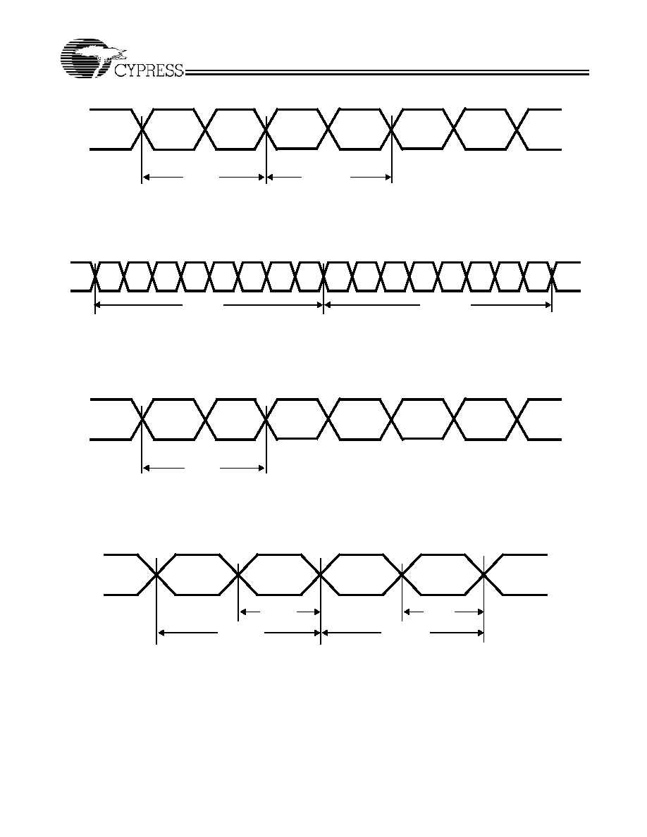
11. Lock Time shown in Figure 2.
12. LCLK and 54MOUT Cycle-Cycle Jitter shown in Figure 3.
13. LCLK and 54MOUT 1000 Cycle Jitter shown in Figure 4.
14. CLK/CLKB 1-6 Cycle Jitter specification is absolute value of worst case deviation, and is shown in Figure 5 and Figure 6.
15. CLK/CLKB Long Term Jitter shown in Figure 7.
16. CLK/CLKB Duty Cycle Error shown in Figure 8.

CY22313
Document #: 38-07434 Rev. *E
Page 5 of 9
CLK
CLKB
Vx
Figure 1. Direct Rambus Crossing Point Voltage
VDD
80%
Output stable within PPM spec.
t
5
Figure 2. PLL Lock Time
Output
t
cycle,i
t
cycle,i+1
Figure 3. 54MOUT, LCLK Cycle-to-Cycle Jitter
t
6
= t
cycle,i -
t
cycle,i+1
t
1000cycle,i
t
1000cycle,i+1
...
...
Figure 4. 54MOUT, LCLK 1000 Cycle Jitter
1000 cycles
1000 cycles
t
7
= t
1000cycle,i -
t
1000cycle,i+1
CY22313
Document #: 38-07434 Rev. *E
Page 6 of 9
t
CYCLE,i
t
8
= t
CYLCE,i
≠ t
CYCLE,i+1
over 10000 consecutive cycles
CLK
CLKB
t
CYCLE,i+1
Figure 5. CLK, CLKB Cycle-to-Cycle Jitter
t
4CYCLE,i
t
4CYCLE,i+1
t
8
= t
4CYCLE,i
- t
4CYCLE,i+1 over 10000 consecutive cycles
CLK
CLKB
Figure 6. CLK, CLKB 4-Cycle-to-Cycle Jitter
t
CYCLE
t
9
= t
CYCLE,max
≠ t
CYCLE,min
over 10000 cycles
CLK
CLKB
Figure 7. CLK, CLKB Long-term Jitter
t
PW+,i+1
t
10
= t
PW+,i
≠ t
PW+,i+1
CLK
CLKB
t
PW+,i
t
CYCLE,i
t
CYCLE,i+1
Cycle i
Cycle i+1
Figure 8. CLK, CLKB Duty Cycle Error

CY22313
Document #: 38-07434 Rev. *E
Page 7 of 9
Table 1. Direct Rambus Test Circuit Component Values
Parameter
Description
Value
Tolerance
Unit
R
S
Series Resistor
68
±5%
R
P
Parallel Resistor
39
±5%
C
F
Edge-Rate Filter Capacitor
[17]
15
±10%
pF
C
MID
AC Ground Capacitor
0.01
±20%
µF
R
S
R
S
R
P
R
P
Z
CH
Z
CH
R
T
= Z
CH
R
T
= Z
CH
Measurement Point
Measurement Point
22313
C
F
C
F
C
MID
C
MID
Figure 9. Direct Rambus Test Circuit
0.1
µF
All V
DD
CLK out
C
LOAD
GND
OUTPUTS
Figure 10. LCLK, 54MOUT Output Test Circuits
Ordering Information
Ordering Code
Package
Name
Package Type
Operating Range
Operating Voltages
CY22313ZC
Z24
24-lead TSSOP
Commercial (T
A
= 0
∞C to 85∞C)
3.45V
CY22313ZCT
Z24
24-lead TSSOP ≠ Tape and Reel
Commercial (T
A
= 0
∞C to 85∞C)
3.45V
Lead Free
CY22313ZXC
Z24
24-lead TSSOP
Commercial (T
A
= 0
∞C to 85∞C)
3.45
CY22313ZXCT
Z24
24-lead TSSOP
- Tape and Reel Commercial (T
A
= 0
∞C to 85∞C)
3.45
Notes:
17. CF is OPTIONAL filter capacitor for adjusting edge rates and EMI. No filter capacitors are used for characterization and test data.

CY22313
Document #: 38-07434 Rev. *E
Page 8 of 9
© Cypress Semiconductor Corporation, 2004. The information contained herein is subject to change without notice. Cypress Semiconductor Corporation assumes no responsibility for the use
of any circuitry other than circuitry embodied in a Cypress product. Nor does it convey or imply any license under patent or other rights. Cypress products are not warranted nor intended to be
used for medical, life support, life saving, critical control or safety applications, unless pursuant to an express written agreement with Cypress. Furthermore, Cypress does not authorize its
products for use as critical components in life-support systems where a malfunction or failure may reasonably be expected to result in significant injury to the user. The inclusion of Cypress
products in life-support systems application implies that the manufacturer assumes all risk of such use and in doing so indemnifies Cypress against all charges.
Package Drawing and Dimensions
Rambus is a registered trademark, and Direct Rambus is a trademark, of Rambus Inc. All product and company names mentioned
in this document are the trademarks of their respective holders.
PIN 1 ID
SEATING
PLANE
BSC.
BSC
0∞-8∞
PLANE
GAUGE
1
24
7.70[0.303]
1.10[0.043] MAX.
0.65[0.025]
0.20[0.008]
0.05[0.002]
6.50[0.256]
0.076[0.003]
6.25[0.246]
4.50[0.177]
4.30[0.169]
7.90[0.311]
0.15[0.006]
0.19[0.007]
0.30[0.012]
0.09[[0.003]
0.25[0.010]
0.70[0.027]
0.50[0.020]
0.95[0.037]
0.85[0.033]
24-Lead Thin Shrunk Small Outline Package (4.40-mm Body) Z24
51-85119-*A
DIMENSION IN MM(INCHES)

CY22313
Document #: 38-07434 Rev. *E
Page 9 of 9
Document History Page
Document Title: CY22313 Two-PLL Clock Generator with Direct RambusTM (Lite) Support
Document Number: 38-07434
REV.
ECN NO.
Issue
Date
Orig. of
Change
Description of Change
**
117092
07/02/02
CKN
New Data Sheet
*A
121365
11/15/02
CKN
Reordered Pin Description table
Changed all 3.3V references to 3.45V
Changed RI_FS min. spec to 60 KOhms
Changed note 4
Inserted max. spec for Edge Rates
Reduced min. spec for Edge Rates on 1.8V and 1.675V outputs
Inserted phase noise specifications
Created separate specs for Jitter, depending on output voltage
Correctly specified CF in Table 1
*B
121773
02/17/03
CKN
Added t
PU
row to the Recommended Operating Conditions table
*C
125454
05/19/03
CKN
Updated Switching Characteristics table
Added CY22313LF ordering information and corresponding note
*D
127393
06/12/03
RGL
Removed "PRELIMINARY"
Rephrased Note 18 to provide clarity on marking
*E
239051
See ECN
RGL
Corrected the Lead Free Coding in the Ordering Information table