 | –≠–ª–µ–∫—Ç—Ä–æ–Ω–Ω—ã–π –∫–æ–º–ø–æ–Ω–µ–Ω—Ç: CY22381SI | –°–∫–∞—á–∞—Ç—å:  PDF PDF  ZIP ZIP |

Three-PLL General Purpose FLASH
Programmable Clock Generator
CY22381
Cypress Semiconductor Corporation
∑
3901 North First Street
∑
San Jose
,
CA 95134
∑
408-943-2600
Document #: 38-07012 Rev. *D
Revised October 13, 2004
Features
∑ Three integrated phase-locked loops
∑ Ultra-wide divide counters (eight-bit Q, eleven-bit P, and
seven-bit post divide)
∑ Improved linear crystal load capacitors
∑ Flash programmability
∑ Field programmability
∑ Low-jitter, high-accuracy outputs
∑ Power-management options (Shutdown, OE, Suspend)
∑ Configurable crystal drive strength
∑ Frequency select option via external LVTTL Input
∑ 3.3V operation
∑ Eight-pin SOIC package
∑ CyClocks RTTM support
Benefits
∑ Generates up to three unique frequencies on three
outputs up to 200 MHz from an external source.
Functional upgrade for current CY2081 family.
∑ Allows for 0 ppm frequency generation and frequency
conversion under the most demanding applications
∑ Improves frequency accuracy over temperature, age,
process, and initial offset
∑ Non-volatile programming enables easy customi-
zation, ultra-fast turnaround, performance tweaking,
design timing margin testing, inventory control, lower
part count, and more secure product supply. Can also
be programmed multiple times which reduces
programming errors and provides an easy upgrade
path for existing designs
∑ In-house programming of samples and prototype
quantities is available using the CY3672 FTG devel-
opment Kit. Production quantities are available through
Cypress's value-added distribution partners or by
using third party programmers from BP Microsystems,
HiLo Systems, and others.
∑ Performance suitable for high-end multimedia, commu-
nications, industrial, A/D converters, and consumer
applications
∑ Supports numerous low-power application schemes
and reduces EMI by allowing unused outputs to be
turned off
∑ Adjust crystal drive strength for compatibility with
virtually all crystals
∑ External frequency select option for PLL1, CLKA, and
CLKB
∑ Industry standard supply voltage
∑ Industry standard packaging saves on board space
∑ Easy-to-use software support for design entry
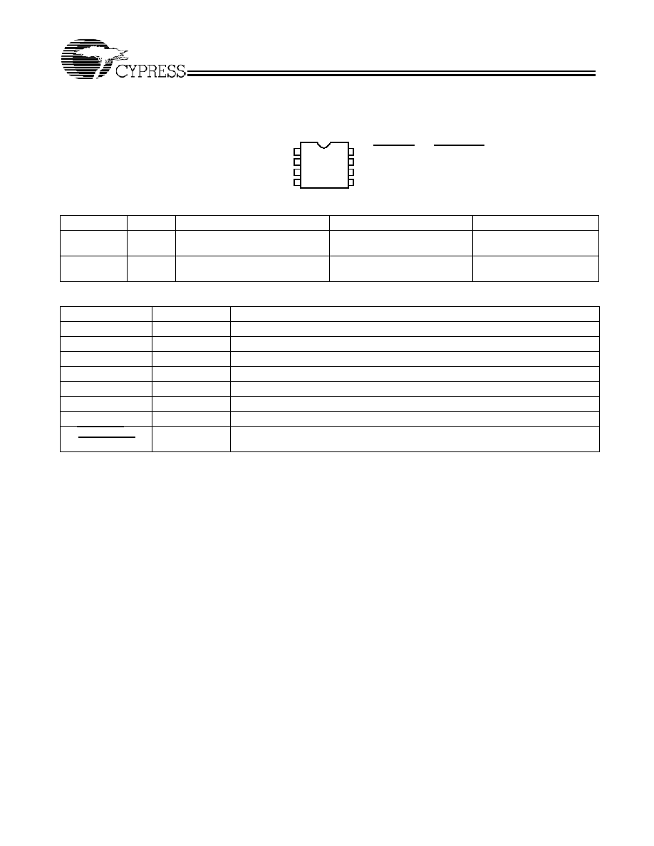
Logic Block Diagram
XTALIN
XTALOUT
FS/SUSPEND
SHUTDOWN/OE
CONFIGURATION
FLASH
OSC.
PLL1
11-BIT P
8-BIT Q
PLL2
11-BIT P
8-BIT Q
PLL3
11-BIT P
8-BIT Q
4 ◊ 3
Switch
Crosspoint
Divider
7-BIT
Divider
7-BIT
Divider
7-BIT
CLKA
CLKB
CLKC
CY22381
Document #: 38-07012 Rev. *D
Page 2 of 8
Pin Configuration
Operation
The CY22381 is an upgrade to the existing CY2081. The new
device has a wider frequency range, greater flexibility,
improved performance, and incorporates many features that
reduce PLL sensitivity to external system issues.
The device has three PLLs that allow each output to operate
at an independent frequencies. These three PLLs are
completely programmable.
Configurable PLLs
PLL1 generates a frequency that is equal to the reference
divided by an eight-bit divider (Q) and multiplied by an 11-bit
divider in the PLL feedback loop (P). The output of PLL1 is sent
to the crosspoint switch. The frequency of PLL1 can optionally
be changed by using the external CMOS general purpose
input. See the following section on "General-Purpose Input" for
more detail.
PLL2 generates a frequency that is equal to the reference
divided by an eight-bit divider (Q) and multiplied by an 11-bit
divider in the PLL feedback loop (P). The output of PLL2 is sent
to the crosspoint switch.
PLL3 generates a frequency that is equal to the reference
divided by an eight-bit divider (Q) and multiplied by an 11-bit
divider in the PLL feedback loop (P). The output of PLL3 is sent
to the cross-point switch.
General-Purpose Input
The CY22381 features an output control pin (pin 8) that can
be programmed to control one of four features.
When programmed as a Frequency Select (FS), the input can
select between two arbitrarily programmed frequency settings.
The Frequency Select can change the following; the frequency
of PLL1, the output divider of CLKB, and the output divider of
CLKA. Any divider change as a result of switching the FS input
is guaranteed to be glitch free.
The general-purpose input can simultaneously control the
Suspend feature, turning off a set of PLLs and outputs deter-
mined during programming.
When programmed as an Output Enable (OE) the input forces
all outputs to be placed in a three-state condition when LOW.
When programmed as a Shutdown, the input forces a full chip
shutdown mode when LOW.
Crystal Input
The input crystal oscillator is an important feature of this device
because of its flexibility and performance features.
The oscillator inverter has programmable drive strength. This
allows for maximum compatibility with crystals from various
manufacturers, processes, performances, and qualities.
The input load capacitors are placed on-die to reduce external
component cost. These capacitors are true parallel-plate
capacitors for ultra-linear performance. These were chosen to
reduce the frequency shift that occurs when non-linear load
Selector Guide
Part Number Outputs
Input Frequency Range
Output Frequency Range
Specifics
CY22381FC
3
8 MHz ≠ 30 MHz (external crystal)
1 MHz ≠ 166 MHz (reference clock)
Up to 200 MHz
Commercial Temperature
CY22381FI
3
8 MHz ≠ 30 MHz (external crystal)
1 MHz ≠ 150 MHz (reference clock)
Up to 166 MHz
Industrial Temperature
Pin Summary
Name
Pin Number
Description
CLKC
1
Configurable clock output C
GND
2
Ground
XTALIN
3
Reference crystal input or external reference clock input
XTALOUT
4
Reference crystal feedback (float if XTALIN is driven by external reference clock)
CLKB
5
Configurable clock output B
CLKA
6
Configurable clock output A
V
DD
7
Power supply
FS/SUSPEND/
OE/SHUTDOWN
8
General Purpose Input. Can be Frequency Control, Suspend mode control, Output
Enable, or full-chip shutdown.
1
2
3
4
5
6
7
8
CLKC
GND
XTALIN
XTALOUT
FS/
SUSPEND
/OE/
SHUTDOWN
V
DD
CLKA
CLKB
8-pin SOIC
CY22381

CY22381
Document #: 38-07012 Rev. *D
Page 3 of 8
capacitance interacts with load, bias, supply, and temperature
changes. Non-linear (FET gate) crystal load capacitors should
not be used for MPEG, POTS dial tone, communications, or
other applications that are sensitive to absolute frequency
requirements.
The value of the load capacitors is determined by six bits in a
programmable register. The load capacitance can be set with
a resolution of 0.375 pF for a total crystal load range of 6 pF
to 30 pF.
For driven clock inputs the input load capacitors may be
completely bypassed. This enables the clock chip to accept
driven frequency inputs up to 166 MHz. If the application
requires a driven input, then XTALOUT must be left floating.
Output Configuration
Under normal operation there are four internal frequency
sources that may be routed via a programmable crosspoint
switch to any of the three outputs via programmable seven-bit
output dividers. The four sources are: reference, PLL1, PLL2,
and PLL3. The following is a description of each output.
CLKA's output originates from the crosspoint switch and goes
through a programmable seven-bit post divider. The seven-bit
post divider derives its value from one of two programmable
registers controlled by FS.
CLKB's output originates from the crosspoint switch and goes
through a programmable seven-bit post divider. The seven-bit
post divider derives its value from one of two programmable
registers controlled by FS.
CLKC's output originates from the crosspoint switch and goes
through a programmable seven-bit post divider. The seven-bit
post divider derives its value from one programmable register.
The Clock outputs have been designed to drive a single point
load with a total lumped load capacitance of 15 pF. While
driving multiple loads is possible with the proper termination,
it is generally not recommended.
Power-Saving Features
When configured as OE, the general-purpose input
three-states all outputs when pulled LOW. When configured as
Shutdown, a LOW on this pin three-states all outputs and
shuts off the PLLs, counters, the reference oscillator, and all
other active components. The resulting current on the V
DD
pins will be less than 5
µA (typical). After leaving shutdown
mode, the PLLs will have to relock.
When configured as SUSPEND, the general-purpose input
can be configured to shut down a customizable set of outputs
and/or PLLs, when LOW. All PLLs and any of the outputs can
be shut off in nearly any combination. The only limitation is that
if a PLL is shut off, all outputs derived from it must also be shut
off. Suspending a PLL shuts off all associated logic, while
suspending an output forces a three-state condition.
Improving Jitter
Jitter Optimization Control is useful in mitigating problems
related to similar clocks switching at the same moment and
causing excess jitter. If one PLL is driving more than one
output, the negative phase of the PLL can be selected for one
of the outputs. This prevents the output edges from aligning,
allowing superior jitter performance.
CyClocks RT Software
CyClocks RT is our second-generation application that allows
users to configure this device. The easy-to-use interface offers
complete control of the many features of this family including
input frequency, PLL and output frequencies, and different
functional options. Data sheet frequency range limitations are
checked and performance tuning is automatically applied. You
can download a free copy of CyClocks RT on Cypress's web
site at http://www.cypress.com.
CY22381
Document #: 38-07012 Rev. *D
Page 4 of 8
Maximum Ratings
(Above which the useful life may be impaired. For user guide-
lines, not tested.)
Supply Voltage ............................................... ≠0.5V to +7.0V
DC Input Voltage.............................. ≠0.5V to + (V
DD
+ 0.5V)
Storage Temperature ..................................≠65∞C to +125∞C
Junction Temperature .................................................. 125∞C
Data Retention @ Tj = 125∞C................................> 10 years
Maximum Programming Cycles........................................100
Package Power Dissipation...................................... 250 mW
Static Discharge Voltage
(per MIL-STD-883, Method 3015) ...........................
2000V
Latch up (per JEDEC 17) ....................................
±200 mA
Operating Conditions
[1]
Parameter
Description
Min.
Typ.
Max.
Unit
V
DD
Supply Voltage
3.135
3.3
3.465
V
T
A
Commercial Operating Temperature, Ambient
0
≠
+70
∞C
Industrial Operating Temperature, Ambient
≠40
≠
+85
∞C
C
LOAD_OUT
Max. Load Capacitance
≠
≠
15
pF
f
REF
External Reference Crystal
8
≠
30
MHz
External Reference Clock
[2]
, Commercial
1
≠
166
MHz
External Reference Clock
[2]
, Industrial
1
≠
150
MHz
t
PU
Power-up time for all VDD's to reach minimum specified voltage
(power ramps must be monotonic)
0.05
≠
500
ms
Electrical Characteristics
Parameter
Description
Conditions
Min.
Typ.
Max.
Unit
I
OH
Output High Current
[3]
V
OH
= V
DD
≠ 0.5, V
DD
= 3.3 V
12
24
≠
mA
I
OL
Output Low Current
[3]
V
OL
= 0.5V, V
DD
= 3.3 V
12
24
≠
mA
C
XTAL_MIN
Crystal Load Capacitance
[3]
Capload at minimum setting
≠
6
≠
pF
C
XTAL_MAX
Crystal Load Capacitance
[3]
Capload at maximum setting
≠
30
≠
pF
C
IN
Input Pin Capacitance
[3]
Except crystal pins
≠
7
≠
pF
V
IH
HIGH-level Input Voltage
CMOS levels,% of V
DD
70%
≠
≠
V
DD
V
IL
LOW-level Input Voltage
CMOS levels,% of V
DD
≠
≠
30%
V
DD
I
IH
Input HIGH Current
V
IN
= V
DD
≠ 0.3 V
≠
<1
10
µA
I
IL
Input LOW Current
V
IN
= +0.3 V
≠
<1
10
µA
I
OZ
Output Leakage Current
Three-state outputs
≠
≠
10
µA
I
DD
Total Power Supply Current
3.3 V Power Supply; 3 outputs @ 50 MHz
≠
35
≠
mA
3.3 V Power Supply; 3 outputs @ 166 MHz
≠
70
≠
mA
I
DDS
Total Power Supply Current in
Shutdown Mode
Shut-down active
≠
5
20
µA
Notes:
1. Unless otherwise noted, Electrical and Switching Characteristics are guaranteed across these operating conditions.
2. External input reference clock must have a duty cycle between 40% and 60%, measured at V
DD
/2.
3. Guaranteed by design, not 100% tested.

CY22381
Document #: 38-07012 Rev. *D
Page 5 of 8
Switching Characteristics
Parameter
Name
Description
Min.
Typ.
Max.
Unit
1/t
1
Output Frequency
[3, 4]
Clock output limit, Commercial
≠
≠
200
MHz
Clock output limit, Industrial
≠
≠
166
MHz
t
2
Output Duty Cycle
[3, 5]
Duty cycle for outputs, defined as t
2
˜ t
1
,
Fout < 100 MHz, divider >= 2, measured
at V
DD
/2
45%
50%
55%
Duty cycle for outputs, defined as t
2
˜ t
1
,
Fout > 100 MHz or divider = 1, measured
at V
DD
/2
40%
50%
60%
t
3
Rising Edge Slew Rate
[3]
Output clock rise time, 20% to 80% of V
DD
0.75
1.4
≠
V/ns
t
4
Falling Edge Slew Rate
[3]
Output clock fall time, 20% to 80% of V
DD
0.75
1.4
≠
V/ns
t
5
Output Three-state Timing
[3]
Time for output to enter or leave
three-state mode after SHUTDOWN/OE
switches
≠
150
300
ns
t
6
Clock Jitter
[3, 6]
Peak-to-peak period jitter, CLK outputs
measured at V
DD
/2
≠
200
≠
ps
t
7
Lock Time
[3]
PLL Lock Time from Power-up
≠
1.0
3
ms
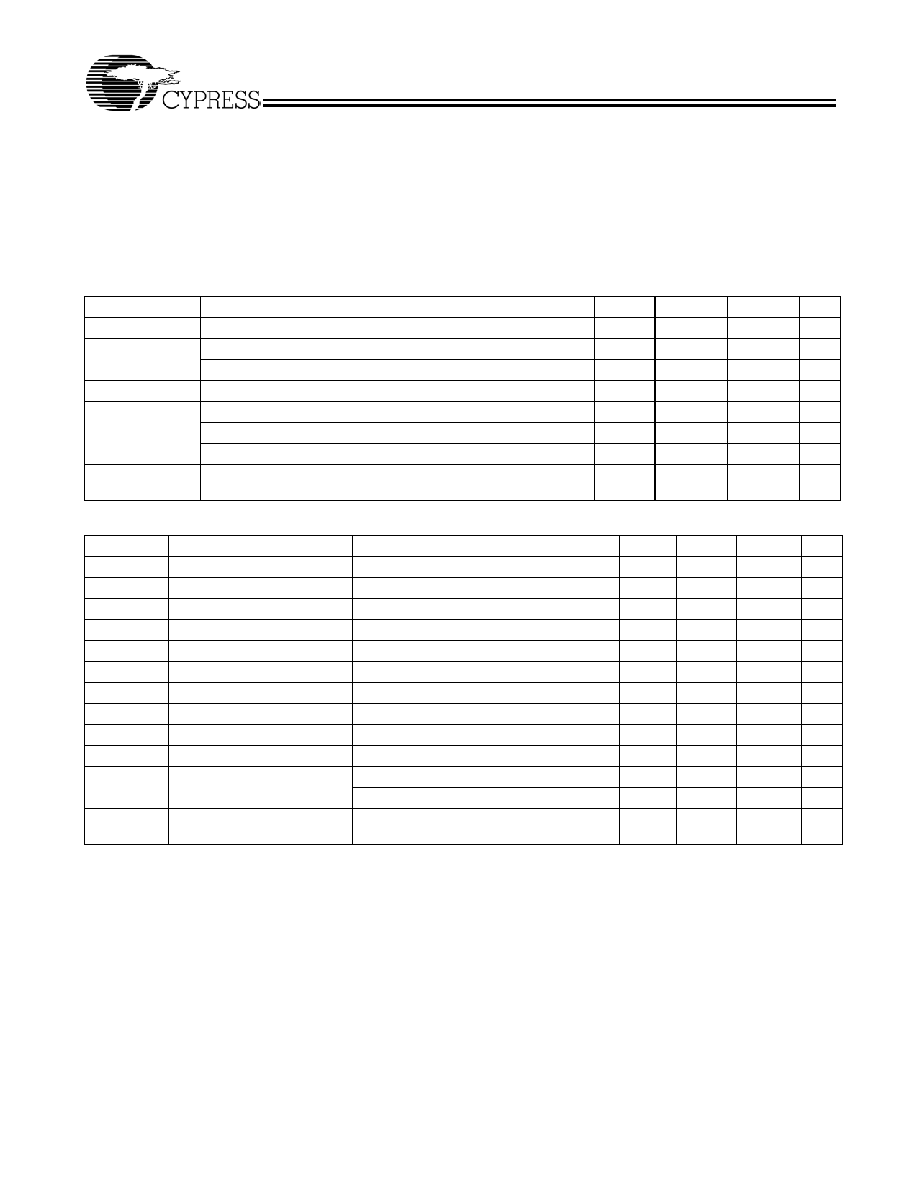
Switching Waveforms
Notes:
4. Guaranteed to meet 20% ≠ 80% output thresholds and duty cycle specifications.
5. Reference Output duty cycle depends on XTALIN duty cycle.
6. Jitter varies significantly with configuration. Reference Output jitter depends on XTALIN jitter and edge rate.
t
1
OUTPUT
t
2
t
3
t
4
All Outputs, Duty Cycle and Rise/Fall Time
t
5
OE
ALL
OUTPUTS
t
5
Output Three-State Timing
THREE-STATE
CLK Output Jitter
CLK
OUTPUT
t
6