Pentium
Æ
/II, 6x86, K6 Clock Synthesizer/Driver for Desktop/
Mobile PCs with Intel
Æ
82430TX and 2 DIMMs or 3 SO-DIMMs
CY2277A
Cypress Semiconductor Corporation
∑
3901 North First Street
∑
San Jose
∑
CA 95134
∑
408-943-2600
Document #: 38-07332 Rev. *A
Revised December 7, 2002
7A
Features
∑ Mixed 2.5V and 3.3V operation
∑ Complete clock solution to meet requirements of Pen-
tium
Æ
, Pentium
Æ
II, 6x86, or K6 motherboards
-- Four CPU clocks at 2.5V or 3.3V
-- Up to eight 3.3V SDRAM clocks
-- Seven 3.3V synchronous PCI clocks, one free
running
-- Two 3.3V USB/IO clocks at 48 or 24 MHz, selectable
by serial interface
-- One 2.5V IOAPIC clock at 14.318 MHz
-- Two 3.3V Ref. clocks at 14.318 MHz
∑ Factory-EPROM programmable CPU, PCI, and USB/IO
clock frequencies for custom configuration
∑ Factory-EPROM programmable output drive and slew
rate for EMI customization
∑ MODE Enable pin for CPU_STOP and PCI_STOP
∑ SMBus serial configuration interface
∑ Available in space-saving 48-pin SSOP and TSSOP
packages.
Functional Description
The CY2277A is a Clock Synthesizer/Driver for Pentium, Pen-
tium II, 6X86, and K6 portable PCs designed with the Intel
Æ
82430TX or similar chipsets. There are three available options
as shown in the selector guide
The CY2277A outputs four CPU clocks at 2.5V or 3.3V with up
to nine selectable frequencies. There are up to eight 3.3V
SDRAM clocks and seven PCI clocks, running at one half the
CPU clock frequency. One of the PCI clocks is free-running.
Additionally, the part outputs two 3.3V USB/IO clocks at 48
MHz or 24 MHz, one 2.5V IOAPIC clock at 14.318 MHz, and
two 3.3V reference clocks at 14.318 MHz. The CPU, PCI,
USB, and IO clock frequencies are factory-EPROM program-
mable for easy customization with fast turnaround times.
The CY2277A has power-down, CPU stop and PCI stop pins
for power management control. The CPU stop and PCI stop
are controlled by the MODE pin. They are multiplexed with
SDRAM clock outputs, and are selected when the MODE pin
is driven LOW. Additionally, these inputs are synchronized
on-chip, enabling glitch-free transitions. When the
CPU_STOP input is asserted, the CPU outputs are driven
LOW. When the PCI_STOP input is asserted, the PCI outputs
(except the free-running PCI clock) are driven LOW. Finally,
when the PWR_DWN pin is asserted, the reference oscillator
and PLLs are shut down, and all outputs are driven LOW.
The CY2277A outputs are designed for low EMI emission.
Controlled rise and fall times, unique output driver circuits and
factory-EPROM programmable output drive and slew-rate en-
able optimal configurations for EMI control.
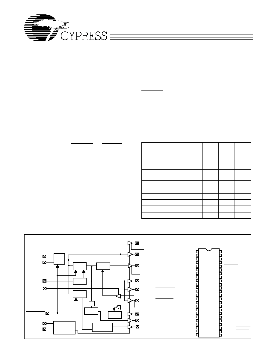
CY2277A Selector Guide
Note:
1.
One free-running PCI clock.
Clock Outputs
-1/-1M
-3
-7M
-12/
-12M/
-12I
CPU (60, 66.6 MHz)
4
--
4
4
CPU (33.3, 66.6 MHz)
--
4
--
--
CPU (SMBus select-
able)
--
--
--
--
PCI (CPU/2)
7
[1]
7
[1]
7
[1]
7
[1]
SDRAM
6/8
6/8
6/8
6/8
USB/IO (48 or 24 MHz)
2
2
2
2
IOAPIC (14.318 MHz)
1
1
1
1
Ref (14.318 MHz)
2
2
2
2
CPU-PCI delay
1≠6 ns
1≠6 ns
<1 ns
1≠4 ns
EPROM
Pin Configuration
Logic Block Diagram
XTALOUT
XTALIN
IOAPIC (14.318 MHz)
14.318
MHz
OSC.
SDRAM[0≠5]
SEL
SDRAM7/PCI_STOP
V
DDQ2
CPU
PLL
MODE
SYS
PLL
/2
Delay
1
2
3
4
5
6
7
8
9
10
11
12
33
32
31
30
29
25
26
27
28
36
35
REF1
34
SSOP
Top View
13
14
15
16
17
18
19
20
21
22
23
24
45
44
43
42
41
37
38
39
40
48
47
46
C
Y
2277
A
-
1,-1M
,
-3,
-
7M
,-12,
-12M
,-12
I
REF0
V
SS
XTALIN
XTALOUT
MODE
V
DDQ3
PCICLK_F
PCICLK0
V
SS
PCICLK1
PCICLK2
PCICLK3
PCICLK4
V
DDQ3
PCICLK5
V
SS
SEL
SDATA
SCLK
V
DDQ3
USBCLK/IOCLK
USBCLK/IOCLK
V
SS
AV
DD
PWR_SEL
V
DDQ2
IOAPIC
PWR_DWN
V
SS
CPUCLK0
CPUCLK1
V
DDCPU
CPUCLK2
CPUCLK3
V
SS
SDRAM0
SDRAM1
V
DDQ3
SDRAM2
SDRAM3
V
SS
SDRAM4
SDRAM5
V
DDQ3
SDRAM6/CPU_STOP
SDRAM7/PCI_STOP
AV
DD
SCLK
SDATA
REF [0≠1]
(14.318)
CPUCLK[0≠3]
V
DDCPU
SDRAM6/CPU_STOP
PCI[0≠5]
PCICLK_F
USBCLK/IOCLK[0:1]
STOP
STOP
INTERFACE
CONTROL
LOGIC
SERIAL
LOGIC
LOGIC
Divide and
Mux Logic
PWR_DWN

CY2277A
Document #: 38-07332 Rev. *A
Page 2 of 19
Pin Summary
Name
Pins
Description
V
DDQ3
7, 15, 21, 28, 34
3.3V Digital voltage supply
V
DDQ2
46
IOAPIC Digital voltage supply, 2.5V
V
DDCPU
40
CPU Digital voltage supply, 2.5V or 3.3V
AV
DD
25, 48
3.3V Analog voltage supply
V
SS
3, 10, 17, 24, 31, 37, 43
Ground
XTALIN
[2]
4
Reference crystal input
XTALOUT
[2]
5
Reference crystal feedback
MODE
6
Mode select input, enables power management features
SEL
18
Select input to enable 66.66 MHz or 60 MHz CPU clock (See Function
tables.)
SDATA
19
SMBus serial data input for serial configuration port
SCLK
20
SMBus serial clock input for serial configuration port
PWR_DWN
44
Active low control input to put osc., PLLs, and outputs in power down state
PWR_SEL
47
Power select input, indicates whether V
DDCPU
is at 2.5V or 3.3V
HIGH = 3.3V, LOW=2.5V (internal pull-up to V
DD
)
SDRAM7/PCI_STOP
26
SDRAM clock output. Also, active LOW control input to stop PCI clocks,
enabled when MODE is LOW
SDRAM6/CPU_STOP
27
SDRAM clock output. Also, active LOW control input to stop CPU clocks,
enabled when MODE is LOW
SDRAM[0:5]
36, 35, 33, 32, 30, 29
SDRAM clock outputs, have same frequency as CPU clocks
CPUCLK[0:3]
42, 41, 39, 38
CPU clock outputs
PCICLK[0:5]
9, 11, 12, 13, 14, 16
PCI clock outputs
PCICLK_F
8
PCI clock output, free-running
IOAPIC
45
IOAPIC clock output
REF[0:1]
1, 2
Reference clock outputs, 14.318 MHz. REF0 drives 45 pF load
USBCLK/IOCLK
22, 23
USB or IO clock outputs, frequency selected by serial word
Note:
2.
For best accuracy, use a parallel-resonant crystal, C
LOAD
= 18 pF.

CY2277A
Document #: 38-07332 Rev. *A
Page 3 of 19
CPU and PCI Clock Driver Strengths
∑ Matched impedances on both rising and falling edges on
the output drivers
∑ Output impedance: 25
(typical) measured at 1.5V
Notes:
3.
On power-up, the default frequency on these outputs is 48 MHz.
4.
Meets Intel USB clock requirements.
Function Table (-1, -1M, -7M, -12, -12M, -12I)
SEL
XTALIN
CPUCLK[0:3]
SDRAM[0:7]
PCICLK[0:5]
PCICLK_F
REF[0:1]
IOAPIC
USBCLK / IOCLK
[3]
0
14.318 MHz
60.0 MHz
30.0 MHz
14.318 MHz
48.0 MHz / 24.0 MHz
1
14.318 MHz
66.67 MHz
33.33 MHz
14.318 MHz
48.0 MHz / 24.0 MHz
Function Table (-3)
SEL
XTALIN
CPUCLK[0:3]
SDRAM[0:7]
PCICLK[0:5]
PCICLK_F
REF[0:1]
IOAPIC
USBCLK / IOCLK
[3]
0
14.318 MHz
33.33 MHz
16.67 MHz
14.318 MHz
48.0 MHz / 24.0 MHz
1
14.318 MHz
66.67 MHz
33.33 MHz
14.318 MHz
48.0 MHz / 24.0 MHz
Actual Clock Frequency Values (-1, -1M, -3, -7M,
-12, -12M, -12I)
Clock Output
Target
Frequency
(MHz)
Actual
Frequency
(MHz)
PPM
CPUCLK,
SDRAM
66.67
66.654
≠195
CPUCLK,
SDRAM
60.0
60.0
0
USBCLK
[4]
48.0
48.008
167
IOCLK
24.0
24.004
167

CY2277A
Document #: 38-07332 Rev. *A
Page 4 of 19
Serial Configuration Map
∑ The Serial bits will be read by the clock driver in the following
order:
Byte 0 - Bits 7, 6, 5, 4, 3, 2, 1, 0
Byte 1 - Bits 7, 6, 5, 4, 3, 2, 1, 0
.
.
Byte N - Bits 7, 6, 5, 4, 3, 2, 1, 0
∑ Reserved and unused bits should be programmed to "0".
∑ SMBus Address for the CY2277A is:
Power Management Logic
CPU_STOP
PCI_STOP
PWR_DWN
CPUCLK
PCICLK
PCICLK_F
Other Clocks
Osc.
PLLs
X
X
0
LOW
LOW
Stopped
Stopped
Off
Off
0
0
1
LOW
LOW
Running
Running
Running
Running
0
1
1
LOW
33/30 MHz
Running
Running
Running
Running
1
0
1
66/60 MHz
LOW
Running
Running
Running
Running
1
1
1
66/60 MHz
33/30 MHz
Running
Running
Running
Running
A6
A5
A4
A3
A2
A1
A0
R/W
1
1
0
1
0
0
1
----
Byte 0: Functional and Frequency Select Clock
Register (1 = Enable, 0 = Disable)
Bit
Pin #
Description
Bit 7 --
(Reserved) drive to `0'
Bit 6 --
(Reserved) drive to `0' on -1, -1M, -3, -7M, -12,
-12M, -12I
Bit 5 --
(Reserved) drive to `0' on -1, -1M, -3, -7M, -12,
-12M, -12I
Bit 4 --
(Reserved) drive to `0' on -1, -1M, -3, -7M, -12,
-12M, -12I
Bit 3 23
48/24 MHz (Frequency Select) 1 = 48 MHz
(default), 0 = 24 MHz
Bit 2 22
48/24 MHz (Frequency Select) 1 = 48 MHz
(default), 0 = 24 MHz
Bit 1
Bit 0
--
Bit 1
1
1
0
0
Bit 0
1 - Three-State (see table below)
0 - N/A
1 - Test Mode (see table below)
0 - Normal Operation
Select Functions
Functional Description
Outputs
CPU
PCI, PCI_F
SDRAM
Ref
IOAPIC
IOCLK
USBCLK
Three-State
Hi-Z
Hi-Z
Hi-Z
Hi-Z
Hi-Z
Hi-Z
Hi-Z
Test Mode
TCLK/2
[5]
TCLK/4
TCLK/2
TCLK
TCLK
TCLK/4
TCLK/2
Note:
5.
TCLK supplied on the XTALIN, PIN 4.

CY2277A
Document #: 38-07332 Rev. *A
Page 5 of 19
Maximum Ratings
(Above which the useful life may be impaired. For user guide-
lines, not tested.)
Supply Voltage ..................................................≠0.5 to +7.0V
Input Voltage ............................................ ≠0.5V to V
DD
+ 0.5
Storage Temperature (Non-Condensing) .... ≠65
∞
C to +150
∞
C
Junction Temperature ............................................... +150
∞
C
Package Power Dissipation.............................................. 1W
Static Discharge Voltage............................................ >2000V
(per MIL-STD-883, Method 3015, like V
DD
pins tied together)
Byte 1: CPU, 24/48 MHz Active/Inactive
Register (1 = Active, 0 = Inactive), Default = Active
Bit
Pin #
Description
Bit 7
23
48/24 MHz (Active/Inactive)
Bit 6
22
48/24 MHz (Active/Inactive)
Bit 5
--
(Reserved) drive to `0'
Bit 4
N/A
Not Used, drive 0
Bit 3
38
CPUCLK3 (Active/Inactive)
Bit 2
39
CPUCLK2 (Active/Inactive)
Bit 1
41
CPUCLK1 (Active/Inactive)
Bit 0
42
CPUCLK0 (Active/Inactive)
Byte 3: SDRAM Active/Inactive
Register (1 = Active, 0 = Inactive), Default = Active
Bit
Pin #
Description
Bit 7
26
SDRAM7 (Active/Inactive)
Bit 6
27
SDRAM6 (Active/Inactive)
Bit 5
29
SDRAM5 (Active/Inactive)
Bit 4
30
SDRAM4 (Active/Inactive)
Bit 3
32
SDRAM3 (Active/Inactive)
Bit 2
33
SDRAM2 (Active/Inactive)
Bit 1
35
SDRAM1 (Active/Inactive)
Bit 0
36
SDRAM0 (Active/Inactive)
Byte 5: Peripheral Active/Inactive
Register (1 = Active, 0 = Inactive), Default = Active
Bit
Pin #
Description
Bit 7
--
(Reserved) drive to `0'
Bit 6
--
(Reserved) drive to `0'
Bit 5
--
(Reserved) drive to `0'
Bit 4
45
IOAPIC (Active/Inactive)
Bit 3
--
(Reserved) drive to `0'
Bit 2
--
(Reserved) drive to `0'
Bit 1
1
REF1 (Active/Inactive)
Bit 0
2
REF0 (Active/Inactive)
Byte 2: PCI Active/Inactive
Register (1 = Active, 0 = Inactive), Default = Active
Bit
Pin #
Description
Bit 7
--
(Reserved) drive to `0'
Bit 6
8
PCICLK_F (Active/Inactive)
Bit 5
16
PCICLK5 (Active/Inactive)
Bit 4
14
PCICLK4 (Active/Inactive)
Bit 3
13
PCICLK3 (Active/Inactive)
Bit 2
12
PCICLK2 (Active/Inactive)
Bit 1
11
PCICLK1 (Active/Inactive)
Bit 0
9
PCICLK0 (Active/Inactive)
Byte 4: SDRAM Active/Inactive
Register (1 = Active, 0 = Inactive), Default = Active
Bit
Pin #
Description
Bit 7
N/A
Not used, drive to `0'
Bit 6
N/A
Not used, drive to `0'
Bit 5
N/A
Not used, drive to `0'
Bit 4
N/A
Not used, drive to `0'
Bit 3
N/A
Not used, drive to `0'
Bit 2
N/A
Not used, drive to `0'
Bit 1
N/A
Not used, drive to `0'
Bit 0
N/A
Not used, drive to `0'
Byte 6: Reserved, for future use