
100-MHz Pentium
ģ
II Clock Synthesizer/Driver with
Spread Spectrum for Mobile or Desktop PCs
CY2280
Cypress Semiconductor Corporation
∑
3901 North First Street
∑
San Jose
∑
CA 95134
∑
408-943-2600
Document #: 38-07207 Rev. *A
Revised December 08, 2002
0
Features
∑ Mixed 2.5V and 3.3V operation
∑ Clock solution for Pentiumģ II, and other similar pro-
cessor-based motherboards
-- Four 2.5V CPU clocks up to 100 MHz
-- Eight 3.3V sync. PCI clocks, one free-running
-- Two 3.3V 48-MHz USB clocks
-- Three 3.3V Ref. clocks at 14.318 MHz
-- Two 2.5V APIC clocks at 14.318 MHz or PCI/2
∑ EMI control
-- Spread spectrum clocking
-- Factory-EPROM programmable spread spectrum
margin
-- Factory-EPROM programmable output drive and
slew rate
∑ Factory-EPROM programmable CPU clock frequencies
for custom configurations
∑ Available in space-saving 48-pin SSOP package
Functional Description
The CY2280 is a Spread Spectrum clock synthesizer/driver for
a Pentium II, or other similar processor-based PC requiring
100-MHz support. All of the required system clocks are provid-
ed in a space-saving 48-pin SSOP package. The CY2280 can
be used with the CY231x for a total solution for systems with
SDRAM.
The CY2280 provides the option of spread spectrum clocking
on the CPU and PCI clocks for reduced EMI. A downspread
percentage is introduced when the SEL_SS input is asserted.
The device can be run without spread spectrum when the
SEL_SS input is deasserted. The percentage of spreading is
EPROM-programmable to optimize EMI-reduction.
The CY2280 has power-down, CPU stop, and PCI stop pins
for power management control. The signals are synchronized
on-chip, and ensure glitch-free transitions on the outputs.
When the CPU_STOP input is asserted, the CPU clock out-
puts are driven LOW. When the PCI_STOP input is asserted,
the PCI clock outputs (except the free-running PCI clock) are
driven LOW. When the PWR_DWN pin is asserted, the refer-
ence oscillator and PLLs are shut down, and all outputs are
driven LOW.
CY2280 Selector Guide
CY2280 Configuration Options
Clock Outputs
≠1
≠11S
≠21S
CPU (66.6, 100 MHz)
4
4
4
PCI (CPU/2, CPU/3)
8
8
8
USB (48 MHz)
2
2
2
APIC (14.318 MHz)
2
2
--
APIC (PCI/2)
--
--
2
Reference (14.318 MHz)
3
3
3
CPU-PCI delay
1.5
-
4.0 ns
1.5
-
4.0 ns
1.5
-
4.0 ns
CPU-APIC delay
--
--
2.0≠4.5 ns
Spread Spectrum (Downspread)
N/A
-
0.6%
-
0.6%
Pentium is a registered trademark of Intel Corporation.
Logic Block Diagram
EPROM
XTALOUT
XTALIN
APIC [0:1]
14.318
MHz
OSC.
SEL0
V
DDAPIC
CPU
PLL
SEL100
Delay
REF [0-2]
CPUCLK [0-3]
V
DDCPU
PCI [1-7]
PCICLK_F
STOP
STOP
LOGIC
LOGIC
SEL1
USBCLK [0:1]
SYS PLL
CPU_STOP
PWR_DWN
Divider
PCI_STOP
V
DDPCI
V
DDPCI
V
DDREF
V
DDUSB
-1
-2
SEL_SS

CY2280
Document #: 38-07207 Rev. *A
Page 2 of 12
Pin Summary
Name
Pins
Description
V
DDPCI
15, 9
3.3V Digital voltage supply for PCI clocks
V
DDUSB
21
3.3V Digital voltage supply for USB clocks
V
DDREF
48
3.3V Digital voltage supply for REF clocks
V
DDAPIC
46
2.5V Digital voltage supply for APIC clocks
V
DDCPU
41, 37
2.5V Digital voltage supply for CPU clocks
AV
DD
33, 19
Analog voltage supply, 3.3V
V
SS
3, 6, 12, 18, 20, 24, 32, 34, 38, 43 Ground
XTALIN
[1]
4
Reference crystal input
XTALOUT
[1]
5
Reference crystal feedback
PCI_STOP
31
Active LOW control input to stop PCI clocks
CPU_STOP
30
Active LOW control input to stop CPU clocks
PWR_DWN
29
Active LOW control input to power down device
SEL_SS
28
Spread spectrum select input (-11S and -21S options)
N/C
28
Spread spectrum select input (-1 option)
SEL0
27
CPU frequency select input, bit 0 (see Function Table)
SEL1
26
CPU frequency select input, bit 1 (see Function Table)
SEL100
25
CPU frequency select input, selects between 100 MHz and 66.6 MHz
(see Function Table)
CPUCLK[0:3]
40, 39, 36, 35
CPU clock outputs
PCICLK[1:7]
8, 10, 11, 13, 14, 16, 17
PCI clock outputs, at one-half or one-third the CPU frequency of 66.6 MHz
or 100 MHz respectively
PCICLK_F
7
Free-running PCI clock output
APIC[0:1]
45, 44
APIC clock outputs
REF[0:2]
1, 2, 47
3.3V Reference clock outputs
USBCLK[0:1]
22, 23
USB clock outputs
RESERVED
42
Reserved
Note:
1.
For best accuracy, use a parallel-resonant crystal, C
LOAD
= 18 pF.
Pin Configurations
1
2
3
4
5
6
7
8
9
10
11
12
33
32
31
30
29
25
26
27
28
36
35
REF0
34
13
14
15
16
17
18
19
20
21
22
23
24
45
44
43
42
41
37
38
39
40
48
47
46
REF1
V
SS
XTALIN
XTALOUT
PCICLK_F
V
SS
PCICLK1
PCICLK2
V
DDPCI
PCICLK3
V
SS
PCICLK4
V
DDPCI
PCICLK5
PCICLK7
V
SS
AV
DD
V
SS
V
DDUSB
USBCLK0
USBCLK1
V
SS
V
DDREF
REF2
V
DDAPIC
APIC0
APIC1
V
SS
RESERVED
V
DDCPU
CPUCLK0
CPUCLK1
V
SS
V
DDCPU
CPUCLK2
CPUCLK3
V
SS
AV
DD
PCI_STOP
PWR_DWN
N/C
SEL0
SEL1
SEL100
CPU_STOP
V
SS
PCICLK6
1
2
3
4
5
6
7
8
9
10
11
12
33
32
31
30
29
25
26
27
28
36
35
REF0
34
13
14
15
16
17
18
19
20
21
22
23
24
45
44
43
42
41
37
38
39
40
48
47
46
REF1
V
SS
XTALIN
XTALOUT
PCICLK_F
V
SS
PCICLK1
PCICLK2
V
DDPCI
PCICLK3
V
SS
PCICLK4
V
DDPCI
PCICLK5
PCICLK7
V
SS
AV
DD
V
SS
V
DDUSB
USBCLK0
USBCLK1
V
SS
V
DDREF
REF2
V
DDAPIC
APIC0
APIC1
V
SS
RESERVED
V
DDCPU
CPUCLK0
CPUCLK1
V
SS
V
DDCPU
CPUCLK2
CPUCLK3
V
SS
AV
DD
PCI_STOP
PWR_DWN
SEL_SS
SEL0
SEL1
SEL100
CPU_STOP
V
SS
PCICLK6
CY2280-1
CY2280-11S
CY2280-21S
48-
pi
n S
S
O
P
(
T
op
V
i
e
w
)
4
8
-pi
n
S
S
OP
(T
op V
i
ew
)

CY2280
Document #: 38-07207 Rev. *A
Page 3 of 12
Function Table (-11S Option)
SEL100
SEL1
SEL0
SEL_SS
[2]
CPU/PCI
Ratio
CPUCLK
PCICLK_F
PCICLK
REF
APIC USBCLK
0
0
0
N/A
2
Hi-Z
Hi-Z
Hi-Z
Hi-Z
Hi-Z
0
0
1
N/A
2
Reserved
Reserved
14.318 MHz
14.318 MHz
48 MHz
0
1
0
N/A
2
Reserved
Reserved
14.318 MHz
14.318 MHz
48 MHz
0
1
1
0 (downspread)
2
66.66 MHz 33.33 MHz
14.318 MHz
14.318 MHz
48 MHz
0
1
1
1 (no spread)
2
66.66 MHz 33.33 MHz
14.318 MHz
14.318 MHz
48 MHz
1
0
0
N/A
3
TCLK/2
TCLK/6
TCLK
[3]
TCLK
[3]
TCLK/2
1
0
1
N/A
3
Reserved
Reserved
14.318 MHz
14.318 MHz
48 MHz
1
1
0
N/A
3
Reserved
Reserved
14.318 MHz
14.318 MHz
48 MHz
1
1
1
0 (downspread)
3
100 MHz
33.33 MHz
14.318 MHz
14.318 MHz
48 MHz
1
1
1
1 (no spread)
3
100 MHz
33.33 MHz
14.318 MHz
14.318 MHz
48 MHz
Function Table (-21S Option)
SEL100
SEL1
SEL0
SEL_SS
[2]
CPU/PCI
Ratio
CPUCLK
PCICLK_F
PCICLK
REF
APIC USBCLK
0
0
0
N/A
2
Hi-Z
Hi-Z
Hi-Z
Hi-Z
Hi-Z
0
0
1
N/A
2
Reserved
Reserved
14.318 MHz
Reserved
48 MHz
0
1
0
N/A
2
Reserved
Reserved
14.318 MHz
Reserved
48 MHz
0
1
1
0 (downspread)
2
66.66 MHz 33.33 MHz
14.318 MHz
16.67 MHz
48 MHz
0
1
1
1 (no spread)
2
66.66 MHz 33.33 MHz
14.318 MHz
16.67 MHz
48 MHz
1
0
0
N/A
3
TCLK/2
TCLK/6
TCLK
[3]
TCLK/12
[3]
TCLK/2
1
0
1
N/A
3
Reserved
Reserved
14.318 MHz
Reserved
48 MHz
1
1
0
N/A
3
Reserved
Reserved
14.318 MHz
Reserved
48 MHz
1
1
1
0 (downspread)
3
100 MHz
33.33 MHz
14.318 MHz
16.67 MHz
48 MHz
1
1
1
1 (no spread)
3
100 MHz
33.33 MHz
14.318 MHz
16.67 MHz
48 MHz
Actual Clock Frequency Values
Clock Output
Target Frequency
(MHz)
Actual Frequency
(MHz)
PPM
CPUCLK
66.67
66.654
≠195
CPUCLK
100
99.77
≠2346
USBCLK
48.0
48.008
167
Power Management Logic
CPU_STOP
PCI_STOP
PWR_DWN
CPUCLK
PCICLK
PCICLK_F
Other
Clocks
Osc.
PLLs
X
X
0
Low
Low
Low
Low
Off
Off
0
0
1
Low
Low
Running
Running
Running Running
0
1
1
Low
Running
Running
Running
Running Running
1
0
1
Running
Low
Running
Running
Running Running
1
1
1
Running
Running
Running
Running
Running Running
Notes:
2.
Target frequency is modulated by percentage shown (max.) when SEL_SS = 0.
3.
TCLK supplied on the XTALIN pin in Test Mode.

CY2280
Document #: 38-07207 Rev. *A
Page 4 of 12
Maximum Ratings
(Above which the useful life may be impaired. For user guide-
lines, not tested.)
Supply Voltage .................................................≠0.5 to + 7.0V
Input Voltage ............................................ ≠0.5V to V
DD
+ 0.5
Storage Temperature (Non-Condensing) ... ≠65
į
C to +150
į
C
Junction Temperature ............................................... +150
į
C
Package Power Dissipation.............................................. 1W
Static Discharge Voltage........................................... > 2000V
(per MIL-STD-883, Method 3015, like V
DD
pins tied together)
Operating Conditions
[4]
Parameter
Description
Min.
Max.
Unit
AV
DD
, V
DDPCI
,
V
DDUSB
, V
DDREF
Analog and Digital Supply Voltage
3.135
3.465
V
V
DDCPU
CPU Supply Voltage
2.375
2.625
V
V
DDAPIC
APIC Supply Voltage
2.375
2.625
V
T
A
Operating Temperature, Ambient
0
70
į
C
C
L
Max. Capacitive Load on
CPUCLK
PCICLK
APIC, REF
USB
20
30
20
20
pF
f
(REF)
Reference Frequency, Oscillator Nominal Value
14.318
14.318
MHz
t
PU
Power-up time for all VDD's to reach minimum specified voltage (power
ramps must be monotonic)
0.05
50
ms
Electrical Characteristics
Over the Operating Range
Parameter
Description
Test Conditions
Min. Max. Unit
V
IH
High-level Input Voltage
Except Crystal Inputs
[5]
2.0
V
V
IL
Low-level Input Voltage
Except Crystal Inputs
[5]
0.8
V
V
OH
High-level Output Voltage
[6]
V
DDCPU
= V
DDAPIC
= 2.375V
I
OH
= 12 mA CPUCLK
2.0
V
I
OH
= 18 mA APIC
V
OL
Low-level Output Voltage
[6]
V
DDCPU
= V
DDAPIC
= 2.375V
I
OL
= 12 mA
CPUCLK
0.4
V
I
OL
= 18 mA
APIC
V
OH
High-level Output Voltage
[6]
V
DDPCI
, AV
DD
, V
DDREF
, V
DDUSB
= 3.135V I
OH
= 14.5 mA PCICLK
2.4
V
I
OH
= 16 mA USBCLK
I
OH
= 16 mA REF
V
OL
Low-level Output Voltage
[6]
V
DDPCI
, AV
DD
, V
DDREF
,
V
DDUSB
= 3.135V I
OL
= 9.4 mA PCICLK
0.4V
V
I
OL
= 9 mA
USBCLK
I
OL
= 9 mA
REF
I
IH
Input High Current
V
IH
= V
DD
≠10
+10
Ķ
A
I
IL
Input Low Current
V
IL
= 0V
10
Ķ
A
I
OZ
Output Leakage Current
Three-state
≠10
+10
Ķ
A
I
DD25
Power Supply Current for
2.5V Clocks
[6]
V
DDCPU
= 2.625V, V
IN
= 0 or V
DD
, Loaded Outputs, CPU = 66.6 MHz
70
mA
I
DD25
Power Supply Current for
2.5V Clocks
[6]
V
DDCPU
= 2.625V, V
IN
= 0 or V
DD
, Loaded Outputs, CPU = 100 MHz
100
mA
I
DD33
Power Supply Current for
3.3V Clocks
[6]
V
DD
= 3.465V, V
IN
= 0 or V
DD
, Loaded Outputs
170
mA
I
DDS
Power-down Current
[6]
Current draw in power-down state
500
Ķ
A

CY2280
Document #: 38-07207 Rev. *A
Page 5 of 12
Notes:
4.
Electrical parameters are guaranteed with these operating conditions.
5.
Crystal Inputs have CMOS thresholds.
6.
Parameter is guaranteed by design and characterization. Not 100% tested in production.
Electrical Characteristics
Over the Operating Range
Parameter
Description
Test Conditions
Min. Max. Unit
Switching Characteristics
[6, 7]
Parameter
Output
Description
Test Conditions
Min.
Typ.
Max.
Unit
t
1
All
Output Duty Cycle
[8]
t
1
= t
1A
ų
t
1B
45
50
55
%
t
2
CPUCLK,
APIC
CPU and APIC Clock
Rising and Falling Edge
Rate
Between 0.4V and 2.0V
-1,-11S,
-21S
1.0
4.0
V/ns
t
2
PCICLK
PCI Clock Rising and
Falling Edge Rate
Between 0.4V and 2.4V
-1,-11S,
-21S
1.0
4.0
V/ns
t
2
USBCLK,
REF
USB, REF Rising and
Falling Edge Rate
Between 0.4V and 2.4V
0.5
2.0
V/ns
t
3
CPUCLK
CPU Clock Rise Time
Between 0.4V and 2.0V
-1,-11S,
-21S
0.4
1.6
ns
t
4
CPUCLK
CPU Clock Fall Time
Between 2.0V and 0.4V
-1,-11S,
-21S
0.4
1.6
ns
t
5
CPUCLK
CPU-CPU Clock Skew
Measured at 1.25V
100
175
ps
t
6
CPUCLK,
PCICLK
CPU-PCI Clock Skew
[9]
Measured at 1.25V for 2.5V
clocks, and at 1.5V for 3.3V
clocks
-1,-11S,
-21S
1.5
4.0
ns
t
7
PCICLK,
PCICLK
PCI-PCI Clock Skew
Measured at 1.5V
250
ps
t
8
CPUCLK,
APIC
CPU-APIC Clock
Skew
[10]
Measured at 1.25V for 2.5V
clocks
-21S
2.0
4.5
ns
t
9
APIC
APIC-APIC Clock Skew
Measured at 1.25V
100
175
ps
t
10
CPUCLK
Cycle-Cycle Clock Jitter
Measured at 1.25V
-1,-11S,
-21S
200
250
ps
t
11
PCICLK
Cycle-Cycle Clock Jitter
Measured at 1.5V
250
500
ps
t
12
CPUCLK,
PCICLK
Power-up Time
CPU, PCI clock stabilization from
power-up
3
ms
Notes:
7.
All parameters specified with loaded outputs.
8.
Duty cycle is measured at 1.5V when V
DD
= 3.3V. When V
DD
= 2.5V, duty cycle is measured at 1.25V.
9.
PCI lags CPU for -11S and -21S options.
10. APIC lags CPU for -21S option.
CY2280
Document #: 38-07207 Rev. *A
Page 6 of 12
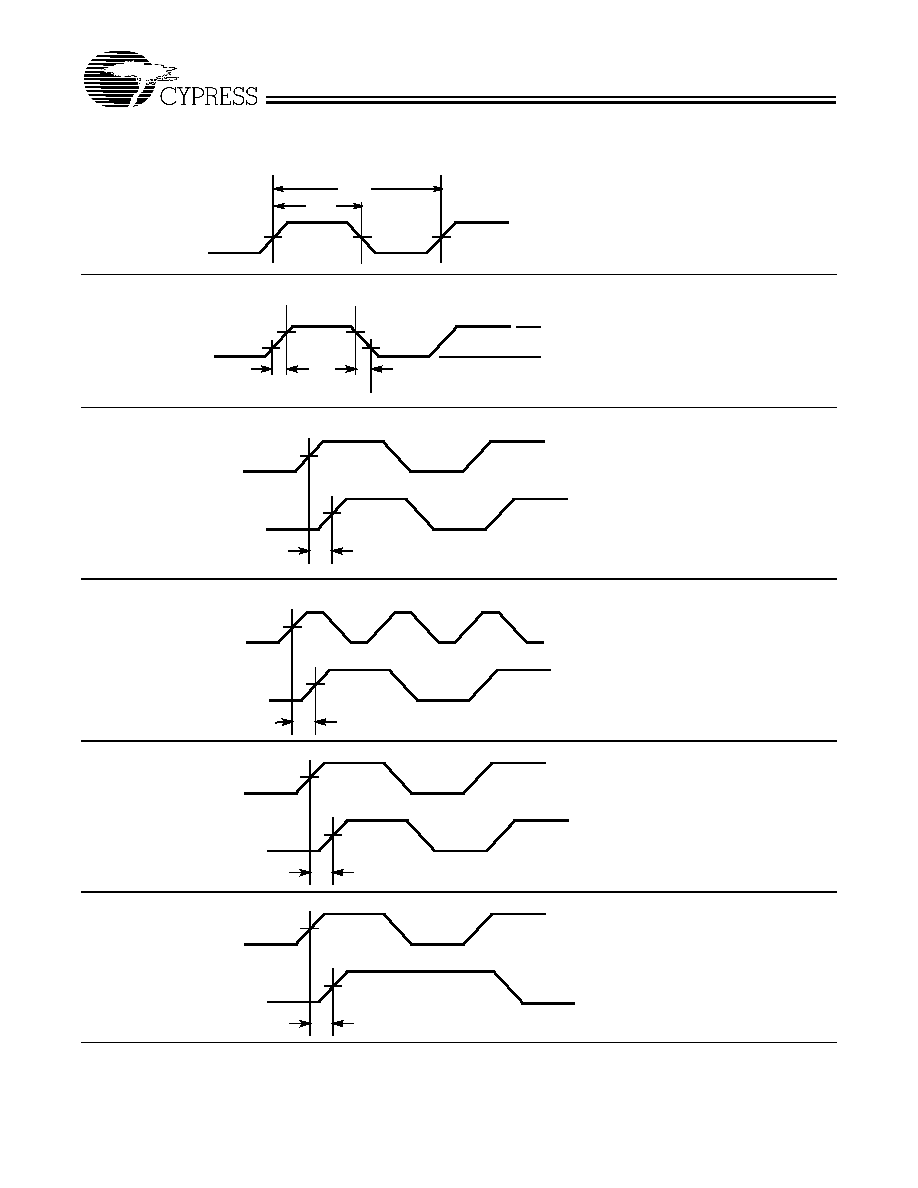
Switching Waveforms
Duty Cycle Timing
t
1A
t
1B
OUTPUT
All Outputs Rise/Fall Time
OUTPUT
t
2
t
3
V
DD
0V
t
2
t
4
CPU-CPU Clock Skew
t
5
CPUCLK
CPUCLK
CPU-PCI Clock Skew
t
6
CPUCLK
PCICLK
t
7
PCICLK
PCICLK
PCI-PCI Clock Skew
t
8
CPUCLK
APIC
CPU-APIC Clock Skew (-21S only)
CY2280
Document #: 38-07207 Rev. *A
Page 7 of 12
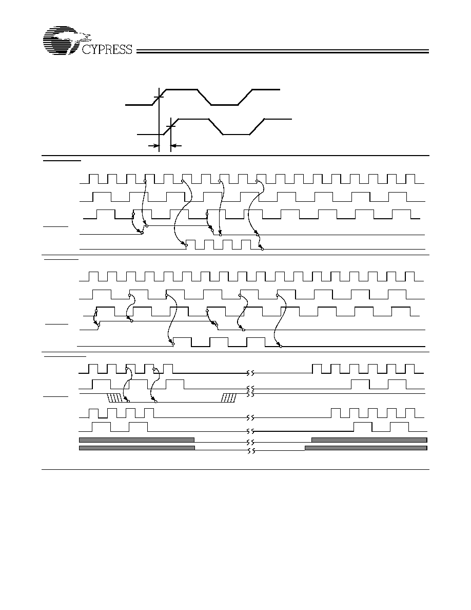
Switching Waveforms
(continued)
t
9
APIC
APIC
APIC-APIC Clock Skew
CPU_STOP
CPUCLK
(Internal)
PCICLK
(Internal)
PCICLK
(Free-Running)
CPU_STOP
CPUCLK
(External)
PCI_STOP
CPUCLK
(Internal)
PCICLK
(Internal)
PCICLK
PCI_STOP
PCICLK
(External)
(Free-Running)
PWR_DOWN
CPUCLK
(Internal)
PCICLK
(Internal)
PWR_DWN
PCICLK
CPUCLK
(External)
(External)
VCO
Crystal
Shaded section on the VCO and Crystal waveforms indicates that the VCO and crystal oscillator are active, and there is a valid clock.
CY2280
Document #: 38-07207 Rev. *A
Page 8 of 12
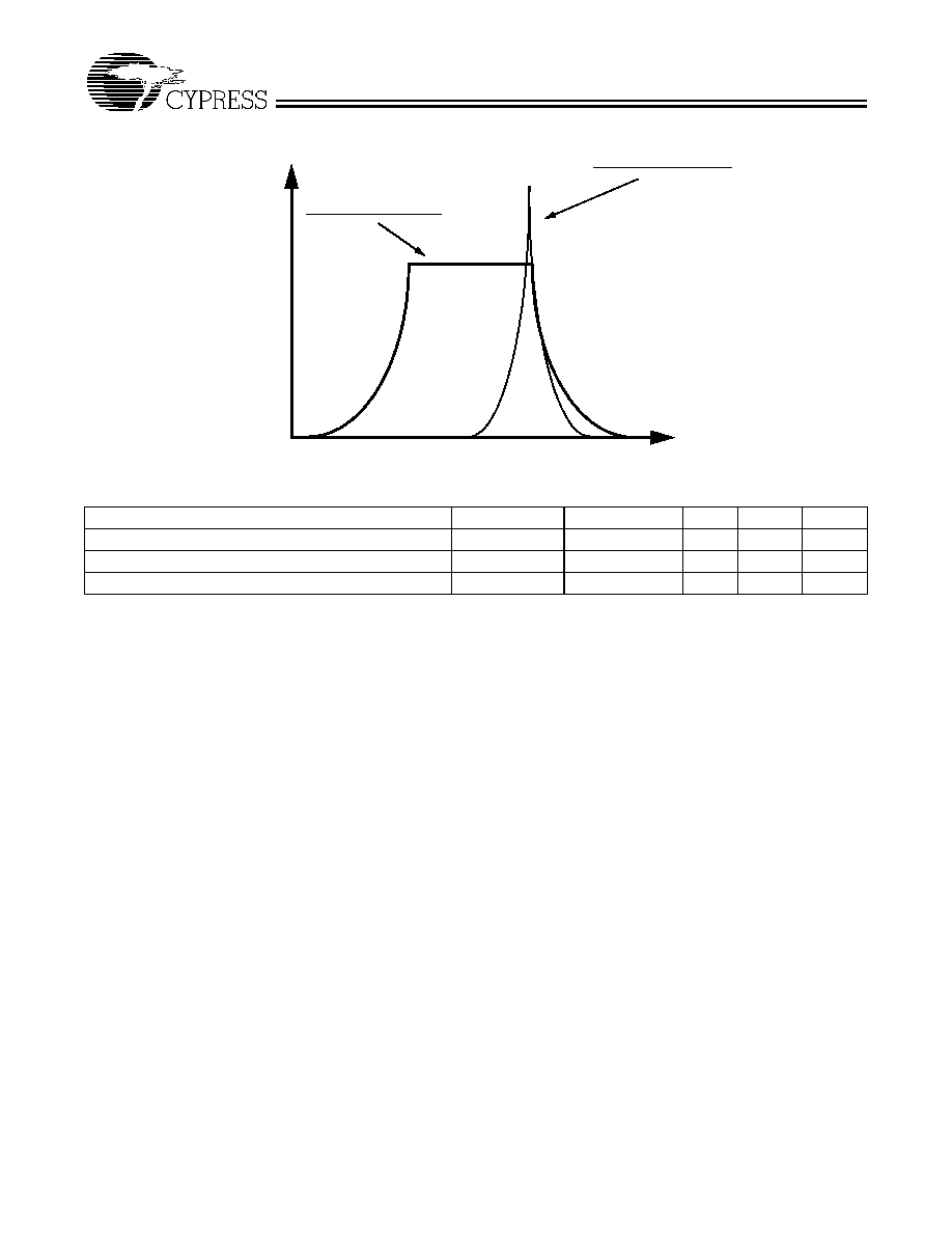
Spread Spectrum Clocking
Frequency (MHz)
Ampli
t
ude (dB
)
Spread Spectrum Enabled
Spread Spectrum Disabled
Description
Configuration
Outputs
Min.
Max.
Unit
Modulation Frequency
All (except -1)
30.0
33.0
kHz
Down Spread Margin at the Fundamental Frequency
-11S
CPU, PCI
0.0
≠0.6
%
Down Spread Margin at the Fundamental Frequency
-21S
CPU, PCI, APIC
0.0
≠0.6
%

CY2280
Document #: 38-07207 Rev. *A
Page 9 of 12
Application Information
Clock traces must be terminated with either series or parallel termination, as is normally done.
Application Circuit
Summary
∑ A parallel-resonant crystal should be used as the reference to the clock generator. The operating frequency and C
LOAD
of
this crystal should be as specified in the data sheet. Optional trimming capacitors may be needed if a crystal with a different
C
LOAD
is used. Footprints must be laid out for flexibility.
∑ Surface mount, low-ESR, ceramic capacitors should be used for filtering. Typically, these capacitors have a value of 0.1
Ķ
F.
In some cases, smaller value capacitors may be required.
∑ The value of the series terminating resistor satisfies the following equation, where Rtrace is the loaded characteristic imped-
ance of the trace, Rout is the output impedance of the clock generator (specified in the data sheet), and Rseries is the series
terminating resistor.
Rseries > Rtrace ≠ Rout
∑ Footprints must be laid out for optional EMI-reducing capacitors, which should be placed as close to the terminating resistor
as is physically possible. Typical values of these capacitors range from 4.7 pF to 22 pF.
∑ A Ferrite Bead may be used to isolate the Board V
DD
from the clock generator V
DD
island. Ensure that the Ferrite Bead offers
greater than 50
impedance at the clock frequency, under loaded DC conditions. Please refer to the application note "Layout
and Termination Techniques for Cypress Clock Generators" for more details.
∑ If a Ferrite Bead is used, a 10
Ķ
F≠22
Ķ
F tantalum bypass capacitor should be placed close to the Ferrite Bead. This capacitor
prevents power supply droop during current surges.

CY2280
Document #: 38-07207 Rev. *A
Page 10 of 12
Test Circuit
3, 6, 12, 18, 20, 24, 32, 34, 38, 43
9, 15, 19, 21, 33, 48
V
DDPCI
, V
DDCORE
,
C
LOAD
OUTPUTS
0.1
Ķ
F
0.1
Ķ
F
V
DDCPU
, V
DDAPIC
Notes:
CY2280
37, 41, 46
Each supply pin must have an individual decoupling capacitor.
All capacitors must be placed as close to the pins as is possible.
V
DDUSB
, V
DDREF
Ordering Information
Ordering Code
Package Name
Package Type
Operating Range
CY2280PVC-1
O48
48-Pin SSOP
Commercial
CY2280PVC-11S
O48
48-Pin SSOP
Commercial
CY2280PVC-21S
O48
48-Pin SSOP
Commercial
CY2280
Document #: 38-07207 Rev. *A
Page 11 of 12
© Cypress Semiconductor Corporation, 2001. The information contained herein is subject to change without notice. Cypress Semiconductor Corporation assumes no responsibility for the use
of any circuitry other than circuitry embodied in a Cypress Semiconductor product. Nor does it convey or imply any license under patent or other rights. Cypress Semiconductor does not authorize
its products for use as critical components in life-support systems where a malfunction or failure may reasonably be expected to result in significant injury to the user. The inclusion of Cypress
Semiconductor products in life-support systems application implies that the manufacturer assumes all risk of such use and in doing so indemnifies Cypress Semiconductor against all charges.
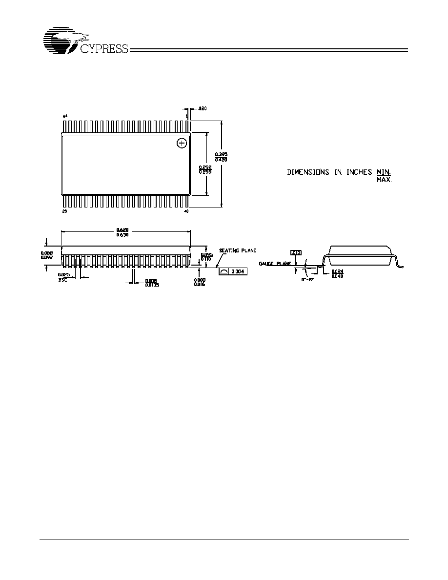
Package Diagram
48-Lead Shrunk Small Outline Package O48
51-85061-B
CY2280
Document #: 38-07207 Rev. *A
Page 12 of 12
Revision History
Document Title: CY2280 100-MHz Pentium
ģ
II Clock Synthesizer/Driver with Spread Spectrum for Mobile or Desktop
PCs
Document Number: 38-07207
REV.
ECN NO.
Issue
Date
Orig. of
Change
Description of Change
**
111721
12/16/01
DSG
Change from Spec number: 38-00694 to 38-07207
*A
121842
12/14/02
RBI
Power up requirements added to Operating Conditions Information