 | –≠–Ľ–Ķ–ļ—ā—Ä–ĺ–Ĺ–Ĺ—č–Ļ –ļ–ĺ–ľ–Ņ–ĺ–Ĺ–Ķ–Ĺ—ā: CY2285 | –°–ļ–į—á–į—ā—Ć:  PDF PDF  ZIP ZIP |

100-MHz Pentium
ģ
II Clock Synthesizer/Driver
with Spread Spectrum for Mobile PCs
CY2285
Cypress Semiconductor Corporation
∑
3901 North First Street
∑
San Jose
∑
CA 95134
∑
408-943-2600
Document #: 38-07205 Rev. *A
Revised December 14, 2002
0
Features
∑ Mixed 2.5V and 3.3V operation
∑ Complete clock solution for Pentium
ģ
II, and other sim-
ilar processor-based motherboards
-- Two CPU clocks at 2.5V up to 100 MHz
-- Six synchronous PCI clocks, one free-running
-- Two 3.3V Reference clocks at 14.318 MHz
-- One 3.3V USB clock running at 48 MHz
-- One 3.3V USB/IO clock running at 48 MHz/24 MHz
∑ Spread Spectrum clocking for EMI control
∑ 1.5≠4.0 ns delay between CPU and PCI clocks
∑ Power-down, CPU stop and PCI stop pins
∑ Low skew outputs,
175 ps between CPU clocks
∑ Early PCI clock leads PCI by 1≠4 ns (-2 option)
∑ DIV4 allows dynamic shifting of CPU and PCI clocks
from the default frequency to default/4 (-2 option)
∑ Factory-EPROM programmable output drive and slew
rate for EMI customization
∑ Available in space-saving 28-pin SSOP package
Functional Description
The CY2285 is a clock synthesizer/driver for Pentium II, or
other similar processor-based mobile PCs requiring up to
100-MHz support. The CY2285 outputs two CPU clocks at
2.5V. There are six PCI clocks, running at one-half or one-third
the CPU clock frequency of 66.6 MHz and 100 MHz respec-
tively. One of the PCI clocks is free-running. Additionally, the
part outputs two 3.3V reference clocks at 14.318 MHz.
The CY2285 incorporates the Intel
ģ
-defined spread spectrum
features. It provides a ≠0.6% downspread on the CPU and PCI
clocks, which can help reduce EMI in certain high-speed sys-
tems.
The CY2285 possesses power-down, CPU stop, and PCI stop
pins for power management control. The signals are synchro-
nized on-chip, and ensure glitch-free transitions on the out-
puts. When the CPU_STOP input is asserted, the CPU clock
outputs are driven LOW. When the PCI_STOP input is assert-
ed, the PCI clock outputs (except the free-running PCI clock)
are driven LOW. When the PWR_DWN pin is asserted, the
reference oscillator and PLLs are shut down, and all outputs
are driven LOW.
The CY2285-2 features an early PCI clock which leads the
other PCI clocks by 1≠4 ns. The CY2285-2 also features a
DIV4 pin which allows for dynamic shifting of CPU and PCI
clocks from the default frequency to the default/4.
Notes:
1.
One free-running PCI clock.
2.
One early PCI clock.
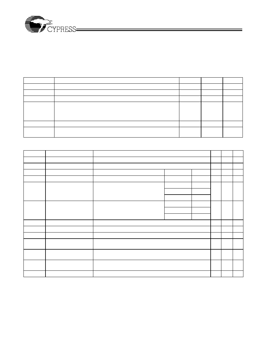
CY2285 Selector Guide
Clock Outputs
CY2285-1
CY2285-2
CY2285-3
CPU (66,
100 MHz)
2
2
2
PCI (CPU/2,
CPU/3 MHz)
6
[1]
7
[1, 2]
6
[1]
Ref. (14.318 MHz)
2
2
1
USB (48 MHz)
1
1
1
USB/IO (48
MHz/24 MHz
selectable)
1
N/A
1
CPU-PCI delay
1.5≠4.0 ns
1.5≠4.0 ns
1.5≠4.0 ns
EPCI-PCI delay
N/A
1.0≠4.0 ns
N/A
Spread Spectrum
≠0.6%
Downsprea
d
≠0.6%
Downsprea
d
≠0.6%
Downsprea
d
Intel and Pentium are registered trademarks of Intel Corporation.
Logic Block Diagram
EPROM
XTALOUT
XTALIN
14.318
MHz
OSC.
CPU
PLL
Delay
REF1/SEL48
CPUCLK [0≠1]
V
DDCPU
PCICLK [1-5]
EPCICLK (-2 option)
STOP
STOP
LOGIC
LOGIC
CPU_STOP
DIV4
Divider
PCI_STOP
V
DDPCI
V
DDPCI
V
DDREF
REF0/SPREAD
SYS
PLL
USBCLK
V
DD48
USB_IOCLK/TS (-1 option)
V
DD48
PCICLK_F
V
DDPCI
PWR_DWN
USBCLK/SEL100/66 (-2 option)
/4
SPREAD (-2,-3 option)
REF0 (-2 option)
REF1 (-2,-3 option)

CY2285
Document #: 38-07205 Rev. *A
Page 2 of 10
Pin Configurations
Pin Summary: CY2285-1, CY2285-3
Name
Pins
Description
V
DD
8, 12, 19, 28
3.3V Power supply voltage
V
DDCPU
25
2.5V Power supply for CPU clocks
V
SS
1, 7, 15, 21, 22
Ground
XTALIN
[3]
2
Reference crystal input
XTALOUT
[3]
3
Reference crystal feedback
PCI_STOP
20
Active LOW control input to stop PCI clocks
CPU_STOP
18
Active LOW control input to stop CPU clocks
PWR_DWN
17
Active LOW control input to power down device
SEL100
16
Select for enabling 100-MHz or 66-MHz CPU clock
HIGH = 100 MHz, LOW = 66 MHz
CPUCLK[0:1]
23, 24
2.5V CPU clock outputs
PCICLK[1:5]
5, 6, 9, 10, 11
3.3V PCI clock outputs
PCICLK_F
4
3.3V Free-running PCI clock output
REF0/SPREAD
26 (-1 option)
3.3V 14.318-MHz reference clock output and power-on spread spectrum
enable strap option.
Strap LOW = Spread Spectrum enable
Strap HIGH = Spread Spectrum disable
SPREAD
26 (-3 option)
Active LOW control input to enable spread spectrum
REF1/SEL48
27
3.3V 14.318-MHz reference clock output and power-on 48-/24-MHz se-
lect strap option.
Strap LOW = 48 MHz on pin14
Strap HIGH = 24 MHz on pin14
USBCLK
13
3.3V 48-MHz USB clock output
USB_IOCLK/TS
14
3.3V 48-MHz or 24-MHz output and three-state strapping option.
Strap LOW = Enter three-state mode for testing
Strap HIGH = Normal Operation
Note:
3.
For best accuracy, use a parallel-resonant crystal, C
LOAD
= 18 pF.
PWRDWN
1
2
3
4
5
6
7
8
9
10
11
12
16
15
SSOP
Top View
13
14
25
24
23
22
21
17
18
19
20
28
27
26
C
Y
2285
-1
V
SSREF
XTAL_IN
PCICLK_F
XTAL_OUT
PCICLK1
V
SSPCI
PCICLK2
V
DDPCI
PCICLK4
V
DD48
PCICLK5
USBCLK
USB_IOCLK/TS
REF1/SEL48
REF0/SPREAD
V
DDCPU
CPUCLK0
CPUCLK1
V
SSCPU
V
SSCORE
V
DDCORE
SEL100
V
SS48
CPU_STOP
PCI_STOP
V
DDREF
PCICLK3
PWRDWN
1
2
3
4
5
6
7
8
9
10
11
12
16
15
SSOP
Top View
13
14
25
24
23
22
21
17
18
19
20
28
27
26
C
Y
2285-
2
REF0
XTAL_IN
PCICLK_F
XTAL_OUT
PCICLK1
V
SSPCI
PCICLK2
V
DDPCI
PCICLK4
EPCICLK
PCICLK5
V
DD48
USBCLK/SEL100/66
REF1
SPREAD
V
DDCPU
CPUCLK0
CPUCLK1
V
SSCPU
V
SSCORE
V
DDCORE
DIV4
V
SS48
CPU_STOP
PCI_STOP
V
DDREF
PCICLK3
PWRDWN
1
2
3
4
5
6
7
8
9
10
11
12
16
15
SSOP
Top View
13
14
25
24
23
22
21
17
18
19
20
28
27
26
C
Y
2
285-
3
V
SSREF
XTAL_IN
PCICLK_F
XTAL_OUT
PCICLK1
V
SSPCI
PCICLK2
V
DDPCI
PCICLK4
V
DD48
PCICLK5
USBCLK
USB_IOCLK/TS
REF1/SEL48
SPREAD
V
DDCPU
CPUCLK0
CPUCLK1
V
SSCPU
V
SSCORE
V
DDCORE
SEL100
V
SS48
CPU_STOP
PCI_STOP
V
DDREF
PCICLK3

CY2285
Document #: 38-07205 Rev. *A
Page 3 of 10
Pin Summary: CY2285-2
Name
Pins
Description
V
DD
8, 13, 19, 28
3.3V Power supply
V
DDCPU
25
2.5V Power supply
V
SS
7, 15, 21, 22
Ground
XTALIN
[3]
2
Reference crystal input
XTALOUT
[3]
3
Reference crystal feedback
PCI_STOP
20
Active LOW control input to stop PCI clocks
CPU_STOP
18
Active LOW control input to stop CPU clocks
PWR_DWN
17
Active LOW control input to power down device
DIV4
16
Active LOW control input to enable divide-by-four option on
CPU and PCI clocks
CPUCLK[0:1]
23, 24
2.5V CPU clock outputs
PCICLK[1:5]
5, 6, 9, 10, 11
3.3V PCI clock outputs
PCICLK_F
4
3.3V Free-running PCI clock output
EPCICLK
12
3.3V Early PCI clock output (Not Free-running)
REF0
1
3.3V 14.318-MHz reference clock output
REF1
27
3.3V 14.318-MHz reference clock output
USBCLK/SEL100/66
14
3.3V 48-MHz USB clock output or select input and frequency
select strap option (use 10-k
external strap resistor)
Strap LOW = 66.6-MHz CPU Frequency
Strap HIGH = 100-MHz CPU Frequency
SPREAD
26
Active LOW control input to enable Spread Spectrum
Actual Clock Frequency Values
Clock Output
Target Frequency
(MHz)
Actual Frequency
(MHz)
PPM
CPUCLK
66.67
66.654
≠240
CPUCLK
100
99.77
≠2300
USB 48-MHz
48
48.008
+167
Power Management Logic
CPU_STOP
PCI_STOP
PWR_DWN
CPUCLK
PCICLK
PCICLK_F
Other
Clocks
Osc.
PLLs
X
X
0
Low
Low
Low
Low
Off
Off
0
0
1
Low
Low
Running
Running
Running Running
0
1
1
Low
Running
Running
Running
Running Running
1
0
1
Running
Low
Running
Running
Running Running
1
1
1
Running
Running
Running
Running
Running Running

CY2285
Document #: 38-07205 Rev. *A
Page 4 of 10
Function Table: CY2285-1
SEL100
SEL48
[4]
TS
[4]
SPREAD
[4]
CPUCLK[0:1]
PCICLK[1:5],
PCICLK_F
USB_IOCLK
USBCLK
REFCLK [0-1]
X
X
0
X
Hi-Z
Hi-Z
Hi-Z
Hi-Z
Hi-Z
0
1
1
1 (no spread)
66.6 MHz
33.3 MHz
24 MHz
48 MHz
14.318 MHz
0
0
1
0 (≠0.6%
downspread)
66.6 MHz
33.3 MHz
48 MHz
48 MHz
14.318 MHz
1
1
1
1 (no spread)
100 MHz
33.3 MHz
24 MHz
48 MHz
14.318 MHz
1
0
1
0 (≠0.6%
downspread)
100 MHz
33.3 MHz
48 MHz
48 MHz
14.318 MHz
Function Table: CY2285-2
SEL100/66
[4]
SPREAD
DIV4
CPUCLK [0:1]
PCICLK[1:5],
PCICLK_F,
EPCICLK
USBCLK
REFCLK[0:1]
0
0 (≠0.6% downspread)
1
66.67 MHz
33.3 MHz
48 MHz
14.318 MHz
0
1 (no spread)
1
66.67 MHz
33.3 MHz
48 MHz
14.318 MHz
1
0 (≠0.6% downspread)
1
100 MHz
33.3 MHz
48 MHz
14.318 MHz
1
1 (no spread)
1
100 MHz
33.3 MHz
48 MHz
14.318 MHz
0
0 (≠0.6% downspread)
0
16.67 MHz
8.33 MHz
48 MHz
14.318 MHz
0
1 (no spread)
0
16.67 MHz
8.33 MHz
48 MHz
14.318 MHz
1
0 (≠0.6% downspread)
0
25.0 MHz
8.33 MHz
48 MHz
14.318 MHz
1
1 (no spread)
0
25.0 MHz
8.33 MHz
48 MHz
14.318 MHz
Function Table: CY2285-3
SEL100
SEL48
[4]
TS
[4]
SPREAD
[4]
CPUCLK[0:1]
PCICLK[1:5],
PCICLK_F
USB_IOCLK
USBCLK
REFCLK1
X
X
0
X
Hi-Z
Hi-Z
Hi-Z
Hi-Z
Hi-Z
0
1
1
1 (no spread)
66.6 MHz
33.3 MHz
24 MHz
48 MHz
14.318 MHz
0
0
1
0 (≠0.6%
downspread)
66.6 MHz
33.3 MHz
48 MHz
48 MHz
14.318 MHz
1
1
1
1 (no spread)
100 MHz
33.3 MHz
24 MHz
48 MHz
14.318 MHz
1
0
1
0 (≠0.6%
downspread)
100 MHz
33.3 MHz
48 MHz
48 MHz
14.318 MHz
Note:
4.
Power-on strap option.
CY2285
Document #: 38-07205 Rev. *A
Page 5 of 10
Maximum Ratings
(Above which the useful life may be impaired. For user guide-
lines, not tested.)
Supply Voltage ..................................................≠0.5 to +7.0V
Input Voltage .............................................. ≠0.5V to V
DD
+0.5
Storage Temperature (Non-Condensing) ... ≠65
į
C to +150
į
C
Junction Temperature ............................................... +150
į
C
Static Discharge Voltage............................................ >2000V
(per MIL-STD-883, Method 3015, like V
DD
pins tied together)
Operating Conditions
[5]
Parameter
Description
Min.
Max.
Unit
V
DD
Analog and Digital 3.3V Supply Voltage
3.135
3.465
V
V
DDCPU
CPU Supply Voltage
2.375
2.625
V
T
A
Operating Temperature, Ambient
0
70
į
C
C
L
Max. Capacitive Load on
CPUCLK
PCICLK
REF
20
30
35
pF
f
(REF)
Reference Frequency, Oscillator Nominal Value
14.318
14.318
MHz
t
PU
Power-up time for all VDD's to reach minimum specified voltage (power
ramps must be monotonic)
0.05
50
ms
Electrical Characteristics
Over the Operating Range
Parameter
Description
Test Conditions
Min. Max. Unit
V
IH
High-level Input Voltage
Except Crystal Inputs
[6]
2.0
V
V
IL
Low-level Input Voltage
Except Crystal Inputs
[6]
0.8
V
V
OH
High-level Output Voltage V
DDCPU
= 2.375V
I
OH
= 12 mA
CPUCLK
2.0
V
V
OL
Low-level Output Voltage
V
DDCPU
= 2.375V
I
OL
= 12 mA
CPUCLK
0.4
V
V
OH
High-level Output Voltage V
DDPCI
, AV
DD
, V
DDREF
= 3.135V
I
OH
= 14.5 mA PCICLK
2.4
V
I
OH
= 16 mA
REF
I
OH
= 36 mA
REF
[7]
V
OL
Low-level Output Voltage
V
DDPCI
, AV
DD
, V
DDREF
= 3.135V
I
OL
= 9.4 mA
PCICLK
0.4V
V
I
OL
= 9 mA
REF
I
OL
= 29 mA
REF
[7]
I
IH
Input High Current
V
IH
= V
DD
≠10
+10
Ķ
A
I
IL
Input Low Current
V
IL
= 0V
10
Ķ
A
I
OZ
Output Leakage Current
Three-state
≠10
+10
Ķ
A
I
DD25
Power Supply Current for
2.5V clocks
V
DDCPU
= 2.625V, V
IN
= 0 or V
DD
, Loaded Outputs, CPU = 66.6 MHz
70
mA
I
DD25
Power Supply Current for
2.5V clocks
V
DDCPU
= 2.625V, V
IN
= 0 or V
DD
, Loaded Outputs, CPU = 100 MHz
100
mA
I
DD33
Power Supply Current for
3.3V clocks
V
DD
= 3.465V, V
IN
= 0 or V
DD
, Loaded Outputs
170
mA
I
DDS
Powerdown Current
Current draw in powerdown state
500
Ķ
A
Notes:
5.
Electrical parameters are guaranteed with these operating conditions.
6.
Crystal Inputs have CMOS thresholds, nominally V
DD
/2.
7.
CY2285-2 option only.

CY2285
Document #: 38-07205 Rev. *A
Page 6 of 10
Switching Characteristics
[8]
Over the Operating Range
Parameter
Output
Description
Test Conditions
Min.
Typ.
Max.
Unit
t
1
All
Output Duty Cycle
[9]
t
1
= t
1A
ų
t
1B
45
50
55
%
t
2
CPUCLK
CPU Clock Rising and
Falling Edge Rate
Between 0.4V and 2.0V
1.0
4.0
V/ns
t
2
PCICLK
PCI Clock Rising and
Falling Edge Rate
Between 0.4V and 2.4V
1.0
4.0
V/ns
t
2
REF
REF Clock Rising and
Falling Edge Rate
Between 0.4V and 2.4V
0.5
2.0
V/ns
t
3
CPUCLK
CPU Clock Rise Time
Between 0.4V and 2.0V
0.4
1.6
ns
t
4
CPUCLK
CPU Clock Fall Time
Between 2.0V and 0.4V
0.4
1.6
ns
t
5
CPUCLK
CPU-CPU Clock Skew
Measured at 1.25V
100
175
ps
t
6
CPUCLK,
PCICLK
CPU-PCI Clock Skew
Measured at 1.25V for 2.5V clocks, and
at 1.5V for 3.3V clocks
1.5
4.0
ns
t
7
PCICLK,
PCICLK
PCI-PCI Clock Skew
Measured at 1.5V
250
ps
t
7
EPCICLK,
PCICLK
EPCI-PCI Clock Skew
[7]
Measured at 1.5V
1.0
4.0
ns
t
10
CPUCLK
Cycle-Cycle Clock Jitter
Measured at 1.25V
700
ps
t
11
PCICLK
Cycle-Cycle Clock Jitter
Measured at 1.5V
500
ps
t
12
CPUCLK,
PCICLK
Power-up Time
CPU and PCI clock stabilization from
power-up
3
ms
t
13
CPUCLK,
PCICLK
/4 Frequency Slew
Time
[7]
Time for CPU, EPCI, and PCI clock
frequency to change from f to f/4 after
select input change
10
25
cycles
Notes:
8.
All parameters specified with loaded outputs.
9.
Duty cycle is measured at 1.5V when V
DD
= 3.3V. When V
DD
= 2.5V, duty cycle is measured at 1.25V.

CY2285
Document #: 38-07205 Rev. *A
Page 7 of 10
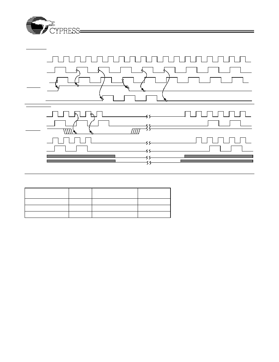
Switching Waveforms
Duty Cycle Timing
t
1A
t
1B
OUTPUT
All Outputs Rise/Fall Time
OUTPUT
t
2
t
3
V
DD
0V
t
2
t
4
CPU-CPU Clock Skew
t
5
CPUCLK
CPUCLK
CPU-PCI Clock Skew
CPUCLK
t
6
PCICLK
t
7
PCI/EPCICLK
PCICLK
PCI/EPCI-PCI Clock Skew
CPUCLK
(Internal)
PCICLK
(Internal)
PCICLK
(Free-Running)
CPU_STOP
CPUCLK
(External)
CPU_STOP
CY2285
Document #: 38-07205 Rev. *A
Page 8 of 10
Switching Waveforms
(continued)
PCI_STOP
CPUCLK
(Internal)
PCICLK
(Internal)
PCICLK
PCI_STOP
PCICLK
(External)
(Free-Running)
PWR_DOWN
CPUCLK
(Internal)
PCICLK
(Internal)
PWR_DWN
PCICLK
CPUCLK
(External)
(External)
VCO
Crystal
Shaded section on the VCO and Crystal waveforms indicates that the VCO and crystal oscillator are active, and there is a valid clock.
Ordering Information
Ordering Code
Package
Name
Package Type
Operating
Range
CY2285PVC-1
O28
28-Pin SSOP
Commercial
CY2285PVC-2
O28
28-Pin SSOP
Commercial
CY2285PVC-3
O28
28-Pin SSOP
Commercial

CY2285
Document #: 38-07205 Rev. *A
Page 9 of 10
© Cypress Semiconductor Corporation, 2001. The information contained herein is subject to change without notice. Cypress Semiconductor Corporation assumes no responsibility for the use
of any circuitry other than circuitry embodied in a Cypress Semiconductor product. Nor does it convey or imply any license under patent or other rights. Cypress Semiconductor does not authorize
its products for use as critical components in life-support systems where a malfunction or failure may reasonably be expected to result in significant injury to the user. The inclusion of Cypress
Semiconductor products in life-support systems application implies that the manufacturer assumes all risk of such use and in doing so indemnifies Cypress Semiconductor against all charges.
Package Diagram
28-Lead (210-Mil) Shrunk Small Outline Package O28
51-85079-C

CY2285
Document #: 38-07205 Rev. *A
Page 10 of 10
Revision History
Document Title: CY2285 100-MHz Pentiumģ II Clock Synthesizer/Driver with Spread Spectrum for Mobile PCs
Document Number: 38-07205
REV.
ECN NO.
Issue
Date
Orig. of
Change
Description of Change
**
111725
12/16/01
DSG
Change from Spec number: 38-00732 to 38-07205
*A
121840
12/14/02
RBI
Power up requirements added to Operating Conditions Information

100-MHz Pentium
ģ
II Clock Synthesizer/Driver
with Spread Spectrum for Mobile PCs
CY2285
Cypress Semiconductor Corporation
∑
3901 North First Street
∑
San Jose
∑
CA 95134
∑
408-943-2600
Document #: 38-07205 Rev. *A
Revised December 14, 2002
0
Features
∑ Mixed 2.5V and 3.3V operation
∑ Complete clock solution for Pentium
ģ
II, and other sim-
ilar processor-based motherboards
-- Two CPU clocks at 2.5V up to 100 MHz
-- Six synchronous PCI clocks, one free-running
-- Two 3.3V Reference clocks at 14.318 MHz
-- One 3.3V USB clock running at 48 MHz
-- One 3.3V USB/IO clock running at 48 MHz/24 MHz
∑ Spread Spectrum clocking for EMI control
∑ 1.5≠4.0 ns delay between CPU and PCI clocks
∑ Power-down, CPU stop and PCI stop pins
∑ Low skew outputs,
175 ps between CPU clocks
∑ Early PCI clock leads PCI by 1≠4 ns (-2 option)
∑ DIV4 allows dynamic shifting of CPU and PCI clocks
from the default frequency to default/4 (-2 option)
∑ Factory-EPROM programmable output drive and slew
rate for EMI customization
∑ Available in space-saving 28-pin SSOP package
Functional Description
The CY2285 is a clock synthesizer/driver for Pentium II, or
other similar processor-based mobile PCs requiring up to
100-MHz support. The CY2285 outputs two CPU clocks at
2.5V. There are six PCI clocks, running at one-half or one-third
the CPU clock frequency of 66.6 MHz and 100 MHz respec-
tively. One of the PCI clocks is free-running. Additionally, the
part outputs two 3.3V reference clocks at 14.318 MHz.
The CY2285 incorporates the Intel
ģ
-defined spread spectrum
features. It provides a ≠0.6% downspread on the CPU and PCI
clocks, which can help reduce EMI in certain high-speed sys-
tems.
The CY2285 possesses power-down, CPU stop, and PCI stop
pins for power management control. The signals are synchro-
nized on-chip, and ensure glitch-free transitions on the out-
puts. When the CPU_STOP input is asserted, the CPU clock
outputs are driven LOW. When the PCI_STOP input is assert-
ed, the PCI clock outputs (except the free-running PCI clock)
are driven LOW. When the PWR_DWN pin is asserted, the
reference oscillator and PLLs are shut down, and all outputs
are driven LOW.
The CY2285-2 features an early PCI clock which leads the
other PCI clocks by 1≠4 ns. The CY2285-2 also features a
DIV4 pin which allows for dynamic shifting of CPU and PCI
clocks from the default frequency to the default/4.
Notes:
1.
One free-running PCI clock.
2.
One early PCI clock.
CY2285 Selector Guide
Clock Outputs
CY2285-1
CY2285-2
CY2285-3
CPU (66,
100 MHz)
2
2
2
PCI (CPU/2,
CPU/3 MHz)
6
[1]
7
[1, 2]
6
[1]
Ref. (14.318 MHz)
2
2
1
USB (48 MHz)
1
1
1
USB/IO (48
MHz/24 MHz
selectable)
1
N/A
1
CPU-PCI delay
1.5≠4.0 ns
1.5≠4.0 ns
1.5≠4.0 ns
EPCI-PCI delay
N/A
1.0≠4.0 ns
N/A
Spread Spectrum
≠0.6%
Downsprea
d
≠0.6%
Downsprea
d
≠0.6%
Downsprea
d
Intel and Pentium are registered trademarks of Intel Corporation.
Logic Block Diagram
EPROM
XTALOUT
XTALIN
14.318
MHz
OSC.
CPU
PLL
Delay
REF1/SEL48
CPUCLK [0≠1]
V
DDCPU
PCICLK [1-5]
EPCICLK (-2 option)
STOP
STOP
LOGIC
LOGIC
CPU_STOP
DIV4
Divider
PCI_STOP
V
DDPCI
V
DDPCI
V
DDREF
REF0/SPREAD
SYS
PLL
USBCLK
V
DD48
USB_IOCLK/TS (-1 option)
V
DD48
PCICLK_F
V
DDPCI
PWR_DWN
USBCLK/SEL100/66 (-2 option)
/4
SPREAD (-2,-3 option)
REF0 (-2 option)
REF1 (-2,-3 option)

CY2285
Document #: 38-07205 Rev. *A
Page 2 of 10
Pin Configurations
Pin Summary: CY2285-1, CY2285-3
Name
Pins
Description
V
DD
8, 12, 19, 28
3.3V Power supply voltage
V
DDCPU
25
2.5V Power supply for CPU clocks
V
SS
1, 7, 15, 21, 22
Ground
XTALIN
[3]
2
Reference crystal input
XTALOUT
[3]
3
Reference crystal feedback
PCI_STOP
20
Active LOW control input to stop PCI clocks
CPU_STOP
18
Active LOW control input to stop CPU clocks
PWR_DWN
17
Active LOW control input to power down device
SEL100
16
Select for enabling 100-MHz or 66-MHz CPU clock
HIGH = 100 MHz, LOW = 66 MHz
CPUCLK[0:1]
23, 24
2.5V CPU clock outputs
PCICLK[1:5]
5, 6, 9, 10, 11
3.3V PCI clock outputs
PCICLK_F
4
3.3V Free-running PCI clock output
REF0/SPREAD
26 (-1 option)
3.3V 14.318-MHz reference clock output and power-on spread spectrum
enable strap option.
Strap LOW = Spread Spectrum enable
Strap HIGH = Spread Spectrum disable
SPREAD
26 (-3 option)
Active LOW control input to enable spread spectrum
REF1/SEL48
27
3.3V 14.318-MHz reference clock output and power-on 48-/24-MHz se-
lect strap option.
Strap LOW = 48 MHz on pin14
Strap HIGH = 24 MHz on pin14
USBCLK
13
3.3V 48-MHz USB clock output
USB_IOCLK/TS
14
3.3V 48-MHz or 24-MHz output and three-state strapping option.
Strap LOW = Enter three-state mode for testing
Strap HIGH = Normal Operation
Note:
3.
For best accuracy, use a parallel-resonant crystal, C
LOAD
= 18 pF.
PWRDWN
1
2
3
4
5
6
7
8
9
10
11
12
16
15
SSOP
Top View
13
14
25
24
23
22
21
17
18
19
20
28
27
26
C
Y
2285
-1
V
SSREF
XTAL_IN
PCICLK_F
XTAL_OUT
PCICLK1
V
SSPCI
PCICLK2
V
DDPCI
PCICLK4
V
DD48
PCICLK5
USBCLK
USB_IOCLK/TS
REF1/SEL48
REF0/SPREAD
V
DDCPU
CPUCLK0
CPUCLK1
V
SSCPU
V
SSCORE
V
DDCORE
SEL100
V
SS48
CPU_STOP
PCI_STOP
V
DDREF
PCICLK3
PWRDWN
1
2
3
4
5
6
7
8
9
10
11
12
16
15
SSOP
Top View
13
14
25
24
23
22
21
17
18
19
20
28
27
26
C
Y
2285-
2
REF0
XTAL_IN
PCICLK_F
XTAL_OUT
PCICLK1
V
SSPCI
PCICLK2
V
DDPCI
PCICLK4
EPCICLK
PCICLK5
V
DD48
USBCLK/SEL100/66
REF1
SPREAD
V
DDCPU
CPUCLK0
CPUCLK1
V
SSCPU
V
SSCORE
V
DDCORE
DIV4
V
SS48
CPU_STOP
PCI_STOP
V
DDREF
PCICLK3
PWRDWN
1
2
3
4
5
6
7
8
9
10
11
12
16
15
SSOP
Top View
13
14
25
24
23
22
21
17
18
19
20
28
27
26
C
Y
2
285-
3
V
SSREF
XTAL_IN
PCICLK_F
XTAL_OUT
PCICLK1
V
SSPCI
PCICLK2
V
DDPCI
PCICLK4
V
DD48
PCICLK5
USBCLK
USB_IOCLK/TS
REF1/SEL48
SPREAD
V
DDCPU
CPUCLK0
CPUCLK1
V
SSCPU
V
SSCORE
V
DDCORE
SEL100
V
SS48
CPU_STOP
PCI_STOP
V
DDREF
PCICLK3

CY2285
Document #: 38-07205 Rev. *A
Page 3 of 10
Pin Summary: CY2285-2
Name
Pins
Description
V
DD
8, 13, 19, 28
3.3V Power supply
V
DDCPU
25
2.5V Power supply
V
SS
7, 15, 21, 22
Ground
XTALIN
[3]
2
Reference crystal input
XTALOUT
[3]
3
Reference crystal feedback
PCI_STOP
20
Active LOW control input to stop PCI clocks
CPU_STOP
18
Active LOW control input to stop CPU clocks
PWR_DWN
17
Active LOW control input to power down device
DIV4
16
Active LOW control input to enable divide-by-four option on
CPU and PCI clocks
CPUCLK[0:1]
23, 24
2.5V CPU clock outputs
PCICLK[1:5]
5, 6, 9, 10, 11
3.3V PCI clock outputs
PCICLK_F
4
3.3V Free-running PCI clock output
EPCICLK
12
3.3V Early PCI clock output (Not Free-running)
REF0
1
3.3V 14.318-MHz reference clock output
REF1
27
3.3V 14.318-MHz reference clock output
USBCLK/SEL100/66
14
3.3V 48-MHz USB clock output or select input and frequency
select strap option (use 10-k
external strap resistor)
Strap LOW = 66.6-MHz CPU Frequency
Strap HIGH = 100-MHz CPU Frequency
SPREAD
26
Active LOW control input to enable Spread Spectrum
Actual Clock Frequency Values
Clock Output
Target Frequency
(MHz)
Actual Frequency
(MHz)
PPM
CPUCLK
66.67
66.654
≠240
CPUCLK
100
99.77
≠2300
USB 48-MHz
48
48.008
+167
Power Management Logic
CPU_STOP
PCI_STOP
PWR_DWN
CPUCLK
PCICLK
PCICLK_F
Other
Clocks
Osc.
PLLs
X
X
0
Low
Low
Low
Low
Off
Off
0
0
1
Low
Low
Running
Running
Running Running
0
1
1
Low
Running
Running
Running
Running Running
1
0
1
Running
Low
Running
Running
Running Running
1
1
1
Running
Running
Running
Running
Running Running

CY2285
Document #: 38-07205 Rev. *A
Page 4 of 10
Function Table: CY2285-1
SEL100
SEL48
[4]
TS
[4]
SPREAD
[4]
CPUCLK[0:1]
PCICLK[1:5],
PCICLK_F
USB_IOCLK
USBCLK
REFCLK [0-1]
X
X
0
X
Hi-Z
Hi-Z
Hi-Z
Hi-Z
Hi-Z
0
1
1
1 (no spread)
66.6 MHz
33.3 MHz
24 MHz
48 MHz
14.318 MHz
0
0
1
0 (≠0.6%
downspread)
66.6 MHz
33.3 MHz
48 MHz
48 MHz
14.318 MHz
1
1
1
1 (no spread)
100 MHz
33.3 MHz
24 MHz
48 MHz
14.318 MHz
1
0
1
0 (≠0.6%
downspread)
100 MHz
33.3 MHz
48 MHz
48 MHz
14.318 MHz
Function Table: CY2285-2
SEL100/66
[4]
SPREAD
DIV4
CPUCLK [0:1]
PCICLK[1:5],
PCICLK_F,
EPCICLK
USBCLK
REFCLK[0:1]
0
0 (≠0.6% downspread)
1
66.67 MHz
33.3 MHz
48 MHz
14.318 MHz
0
1 (no spread)
1
66.67 MHz
33.3 MHz
48 MHz
14.318 MHz
1
0 (≠0.6% downspread)
1
100 MHz
33.3 MHz
48 MHz
14.318 MHz
1
1 (no spread)
1
100 MHz
33.3 MHz
48 MHz
14.318 MHz
0
0 (≠0.6% downspread)
0
16.67 MHz
8.33 MHz
48 MHz
14.318 MHz
0
1 (no spread)
0
16.67 MHz
8.33 MHz
48 MHz
14.318 MHz
1
0 (≠0.6% downspread)
0
25.0 MHz
8.33 MHz
48 MHz
14.318 MHz
1
1 (no spread)
0
25.0 MHz
8.33 MHz
48 MHz
14.318 MHz
Function Table: CY2285-3
SEL100
SEL48
[4]
TS
[4]
SPREAD
[4]
CPUCLK[0:1]
PCICLK[1:5],
PCICLK_F
USB_IOCLK
USBCLK
REFCLK1
X
X
0
X
Hi-Z
Hi-Z
Hi-Z
Hi-Z
Hi-Z
0
1
1
1 (no spread)
66.6 MHz
33.3 MHz
24 MHz
48 MHz
14.318 MHz
0
0
1
0 (≠0.6%
downspread)
66.6 MHz
33.3 MHz
48 MHz
48 MHz
14.318 MHz
1
1
1
1 (no spread)
100 MHz
33.3 MHz
24 MHz
48 MHz
14.318 MHz
1
0
1
0 (≠0.6%
downspread)
100 MHz
33.3 MHz
48 MHz
48 MHz
14.318 MHz
Note:
4.
Power-on strap option.

CY2285
Document #: 38-07205 Rev. *A
Page 5 of 10
Maximum Ratings
(Above which the useful life may be impaired. For user guide-
lines, not tested.)
Supply Voltage ..................................................≠0.5 to +7.0V
Input Voltage .............................................. ≠0.5V to V
DD
+0.5
Storage Temperature (Non-Condensing) ... ≠65
į
C to +150
į
C
Junction Temperature ............................................... +150
į
C
Static Discharge Voltage............................................ >2000V
(per MIL-STD-883, Method 3015, like V
DD
pins tied together)
Operating Conditions
[5]
Parameter
Description
Min.
Max.
Unit
V
DD
Analog and Digital 3.3V Supply Voltage
3.135
3.465
V
V
DDCPU
CPU Supply Voltage
2.375
2.625
V
T
A
Operating Temperature, Ambient
0
70
į
C
C
L
Max. Capacitive Load on
CPUCLK
PCICLK
REF
20
30
35
pF
f
(REF)
Reference Frequency, Oscillator Nominal Value
14.318
14.318
MHz
t
PU
Power-up time for all VDD's to reach minimum specified voltage (power
ramps must be monotonic)
0.05
50
ms
Electrical Characteristics
Over the Operating Range
Parameter
Description
Test Conditions
Min. Max. Unit
V
IH
High-level Input Voltage
Except Crystal Inputs
[6]
2.0
V
V
IL
Low-level Input Voltage
Except Crystal Inputs
[6]
0.8
V
V
OH
High-level Output Voltage V
DDCPU
= 2.375V
I
OH
= 12 mA
CPUCLK
2.0
V
V
OL
Low-level Output Voltage
V
DDCPU
= 2.375V
I
OL
= 12 mA
CPUCLK
0.4
V
V
OH
High-level Output Voltage V
DDPCI
, AV
DD
, V
DDREF
= 3.135V
I
OH
= 14.5 mA PCICLK
2.4
V
I
OH
= 16 mA
REF
I
OH
= 36 mA
REF
[7]
V
OL
Low-level Output Voltage
V
DDPCI
, AV
DD
, V
DDREF
= 3.135V
I
OL
= 9.4 mA
PCICLK
0.4V
V
I
OL
= 9 mA
REF
I
OL
= 29 mA
REF
[7]
I
IH
Input High Current
V
IH
= V
DD
≠10
+10
Ķ
A
I
IL
Input Low Current
V
IL
= 0V
10
Ķ
A
I
OZ
Output Leakage Current
Three-state
≠10
+10
Ķ
A
I
DD25
Power Supply Current for
2.5V clocks
V
DDCPU
= 2.625V, V
IN
= 0 or V
DD
, Loaded Outputs, CPU = 66.6 MHz
70
mA
I
DD25
Power Supply Current for
2.5V clocks
V
DDCPU
= 2.625V, V
IN
= 0 or V
DD
, Loaded Outputs, CPU = 100 MHz
100
mA
I
DD33
Power Supply Current for
3.3V clocks
V
DD
= 3.465V, V
IN
= 0 or V
DD
, Loaded Outputs
170
mA
I
DDS
Powerdown Current
Current draw in powerdown state
500
Ķ
A
Notes:
5.
Electrical parameters are guaranteed with these operating conditions.
6.
Crystal Inputs have CMOS thresholds, nominally V
DD
/2.
7.
CY2285-2 option only.

CY2285
Document #: 38-07205 Rev. *A
Page 6 of 10
Switching Characteristics
[8]
Over the Operating Range
Parameter
Output
Description
Test Conditions
Min.
Typ.
Max.
Unit
t
1
All
Output Duty Cycle
[9]
t
1
= t
1A
ų
t
1B
45
50
55
%
t
2
CPUCLK
CPU Clock Rising and
Falling Edge Rate
Between 0.4V and 2.0V
1.0
4.0
V/ns
t
2
PCICLK
PCI Clock Rising and
Falling Edge Rate
Between 0.4V and 2.4V
1.0
4.0
V/ns
t
2
REF
REF Clock Rising and
Falling Edge Rate
Between 0.4V and 2.4V
0.5
2.0
V/ns
t
3
CPUCLK
CPU Clock Rise Time
Between 0.4V and 2.0V
0.4
1.6
ns
t
4
CPUCLK
CPU Clock Fall Time
Between 2.0V and 0.4V
0.4
1.6
ns
t
5
CPUCLK
CPU-CPU Clock Skew
Measured at 1.25V
100
175
ps
t
6
CPUCLK,
PCICLK
CPU-PCI Clock Skew
Measured at 1.25V for 2.5V clocks, and
at 1.5V for 3.3V clocks
1.5
4.0
ns
t
7
PCICLK,
PCICLK
PCI-PCI Clock Skew
Measured at 1.5V
250
ps
t
7
EPCICLK,
PCICLK
EPCI-PCI Clock Skew
[7]
Measured at 1.5V
1.0
4.0
ns
t
10
CPUCLK
Cycle-Cycle Clock Jitter
Measured at 1.25V
700
ps
t
11
PCICLK
Cycle-Cycle Clock Jitter
Measured at 1.5V
500
ps
t
12
CPUCLK,
PCICLK
Power-up Time
CPU and PCI clock stabilization from
power-up
3
ms
t
13
CPUCLK,
PCICLK
/4 Frequency Slew
Time
[7]
Time for CPU, EPCI, and PCI clock
frequency to change from f to f/4 after
select input change
10
25
cycles
Notes:
8.
All parameters specified with loaded outputs.
9.
Duty cycle is measured at 1.5V when V
DD
= 3.3V. When V
DD
= 2.5V, duty cycle is measured at 1.25V.

CY2285
Document #: 38-07205 Rev. *A
Page 7 of 10
Switching Waveforms
Duty Cycle Timing
t
1A
t
1B
OUTPUT
All Outputs Rise/Fall Time
OUTPUT
t
2
t
3
V
DD
0V
t
2
t
4
CPU-CPU Clock Skew
t
5
CPUCLK
CPUCLK
CPU-PCI Clock Skew
CPUCLK
t
6
PCICLK
t
7
PCI/EPCICLK
PCICLK
PCI/EPCI-PCI Clock Skew
CPUCLK
(Internal)
PCICLK
(Internal)
PCICLK
(Free-Running)
CPU_STOP
CPUCLK
(External)
CPU_STOP

CY2285
Document #: 38-07205 Rev. *A
Page 8 of 10
Switching Waveforms
(continued)
PCI_STOP
CPUCLK
(Internal)
PCICLK
(Internal)
PCICLK
PCI_STOP
PCICLK
(External)
(Free-Running)
PWR_DOWN
CPUCLK
(Internal)
PCICLK
(Internal)
PWR_DWN
PCICLK
CPUCLK
(External)
(External)
VCO
Crystal
Shaded section on the VCO and Crystal waveforms indicates that the VCO and crystal oscillator are active, and there is a valid clock.
Ordering Information
Ordering Code
Package
Name
Package Type
Operating
Range
CY2285PVC-1
O28
28-Pin SSOP
Commercial
CY2285PVC-2
O28
28-Pin SSOP
Commercial
CY2285PVC-3
O28
28-Pin SSOP
Commercial

CY2285
Document #: 38-07205 Rev. *A
Page 9 of 10
© Cypress Semiconductor Corporation, 2001. The information contained herein is subject to change without notice. Cypress Semiconductor Corporation assumes no responsibility for the use
of any circuitry other than circuitry embodied in a Cypress Semiconductor product. Nor does it convey or imply any license under patent or other rights. Cypress Semiconductor does not authorize
its products for use as critical components in life-support systems where a malfunction or failure may reasonably be expected to result in significant injury to the user. The inclusion of Cypress
Semiconductor products in life-support systems application implies that the manufacturer assumes all risk of such use and in doing so indemnifies Cypress Semiconductor against all charges.
Package Diagram
28-Lead (210-Mil) Shrunk Small Outline Package O28
51-85079-C

CY2285
Document #: 38-07205 Rev. *A
Page 10 of 10
Revision History
Document Title: CY2285 100-MHz Pentiumģ II Clock Synthesizer/Driver with Spread Spectrum for Mobile PCs
Document Number: 38-07205
REV.
ECN NO.
Issue
Date
Orig. of
Change
Description of Change
**
111725
12/16/01
DSG
Change from Spec number: 38-00732 to 38-07205
*A
121840
12/14/02
RBI
Power up requirements added to Operating Conditions Information