
20-output, 200-MHz Zero Delay Buffer
CY23020-1
Cypress Semiconductor Corporation
∑
3901 North First Street
∑
San Jose
∑
CA 95134
∑
408-943-2600
Document #: 38-07120 Rev. *B
Revised November 5, 2002
Features
∑ 335 ps max Total Timing BudgetTM (TTB)TM window
∑ 2.5V or 3.3V outputs
∑ 20 LVCMOS outputs
∑ 50 MHz to 200 MHz output frequency
∑ 50 MHz to 200 MHz input frequency
∑ Integrated phase-locked loop (PLL) with lock indicator
∑ Spread AwareTM--designed to work with SSFTG
reference signals
∑ 3.3V core power supply
∑ Available in 48-pin TSSOP and QFN packages
Description
The CY23020-1-1 is a high-performance 200-MHz PLL-based
zero delay buffer designed for high-speed clock distribution
applications. The device features a guaranteed TTB window
specifying all occurrences of output clocks with respect to the
input reference clock across variations in output frequency,
supply voltage, operating temperature, input edge rate, and
process.
The CY23020-1 outputs are three-state when S1 = S2 = 0 for
reduced power. When S1 = 1 and S2 = 0 the PLL is bypassed
and the CY23020-1 functions as a fan-out buffer.
Block Diagram
Pin Configurations
Q2
PLL
Q17
Q18
Q19
FBOUT
FBIN
REF
VDDC
GNDC
REF≠
REF+
VDD
Q19
Q18
GND
Q17
Q16
VDD
Q15
48
47
46
45
44
43
42
41
40
39
38
37
LOCK
NC
FBIN≠
FBIN+
VDD
FBOUT
Q1
GND
Q2
Q3
VDD
Q4
1
2
3
4
5
6
7
8
9
10
11
12
C
Y
230
20-1
Q14
GND
Q13
Q12
VDD
Q11
Q10
GND
GNDC
VDDC
C1
GND
36
35
34
33
32
31
30
29
28
27
26
25
Q5
GND
Q6
Q7
VDD
Q8
Q9
GND
S2
S1
MUL
RANGE
13
14
15
16
17
18
19
20
21
22
23
24
LOCKED
Div
Output
Control
Logic
S1:2
RANGE
MUL
Q1
C1C1
C1
C1
48-pin TSSOP
4 8 - p i n Q F N
4 8
4 7
4 6
4 5
4 4
4 3
4 2
4 1
4 0
3 9
3 8
3 7
1 3
1 4
1 5
1 6
1 7
1 8
1 9
2 0
2 1
2 2
2 3
2 4
1
2
3
4
5
6
7
8
9
1 0
1 1
1 2
3 6
3 5
3 4
3 3
3 2
3 1
3 0
2 9
2 8
2 7
2 6
2 5
F
B
O
U
T
+
V
D
D
F
B
I
N
+
F
B
I
N
-
N
C
L
O
C
K
V
D
D
C
V
S
S
C
R
E
F
-
R
E
F
+
V
D
D
Q
1
9
Q
9
V
S
S
S
2
S
1
M
U
L
R
A
N
G
E
G
N
D
C
1
V
D
D
C
V
S
S
C
V
S
S
Q
1
0
Q 1
V S S
Q 2
Q 3
V D D
Q 4
Q 5
V S S
Q 6
Q 7
V D D
Q 8
Q 1 8
V S S
Q 1 7
Q 1 6
V D D
Q 1 5
Q 1 4
V S S
Q 1 3
Q 1 2
V D D
Q 1 1
CY23020-1
Document #: 38-07120 Rev. *B
Page 2 of 10
Note:
1.
RANGE and MUL have a ~100k pull-down. C1 has a 50k pull-down. These inputs (RANGE, MUL, C1) are static.
2.
There are no power-up sequence requirements on the power supply pins of the CY23020-1.
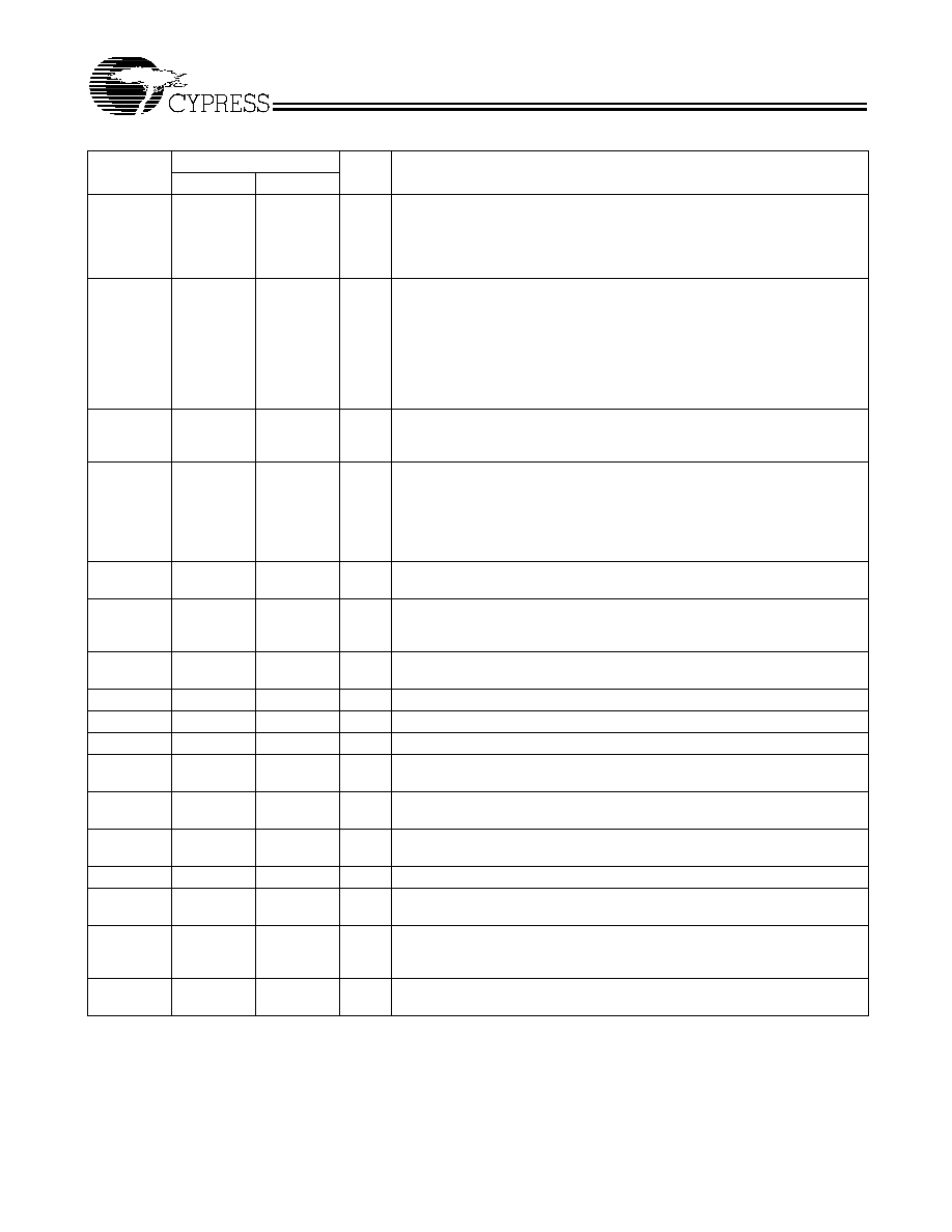
Pin Definitions
[2]
Pin Name
Pin No.
Pin
Type
Pin Description
TSSOP
QFN
REF+
REF≠
45
46
39
40
I
Reference Inputs: Output signals are synchronized to the crossing point of
REF+ and REF≠ signals. Therefore REF≠ must be tied to VREF as defined in
the DC characteristics table. In DC mode, the REF+/REF≠ inputs must be held
at opposite logical states. For optimal performance, the impedances seen by
these two inputs must be equal.
FBIN+
FBIN≠
4
3
46
45
I
Feedback Inputs: Input FBIN+ must be fed by one of the outputs to ensure
proper functionality. If the trace between FBIN+ and FBOUT is equal in length
to the traces between the outputs and the signal destinations, then the signals
received at the destinations will be synchronized to the clock signal at REF+
input.
FBIN≠ must be tied to VREF as defined in the DC characteristics table. In DC
mode, FBIN+/FBIN≠ inputs must be held at opposite logical states. For best
performance, the impedances seen by these two inputs must be equal.
FBOUT
6
48
O
Feedback Output: In order to complete the phase locked loop, an output must
be connected back to the FBIN+ pin. Any of the outputs may actually be used
as the feedback source.
Q1:19
7, 9, 10, 12,
13, 15, 16,
18, 19, 30,
31, 33, 34,
36, 37, 39,
40, 42, 43
1,3,4,6,7,9,1
0,12,13,24,2
5,27,28,30,3
1,33,34,36,3
7
O
Outputs: Refer to Tables 1≠4 for the configuration of these outputs.
RANGE
1
24
18
I
Frequency Range Selection Input: To determine the correct connection for
this pin, refer to Table 2. This should be a static input
LOCK
1
43
O
PLL Locked Output: When this output is HIGH, the PLL in the CY23020-1 is
in steady state operation mode (Locked). When this signal is LOW, the PLL
is in the process of locking onto the reference signal.
S1:2
22, 21
16,15
I
Output/PLL Enable Selection bits: To determine appropriate settings, refer
to Table 1.
VDD
5,11,26, 32
P
Power Connection
VDDC
27, 48
21, 42
P
Analog Power Connection: Connect to 3.3V.
GNDC
28, 47
G
Analog Ground Connection: Connect to common system ground plane.
VDD
5, 11, 17, 32,
38, 44
38,47
P
Output Buffer Power Connections: Connect to 2.5 or 3.3V, whichever is to
be the reference for the output signals.
GND
8, 14, 20, 25,
29, 35, 41
19
G
Ground Connections: Connect to common system ground plane.
VSS
2,8,14,23,29
,35
G
Ground Connections
VSSC
22,41
G
Ground Connections
MUL
[1]
23
17
I
Multiplication Factor Select: When set HIGH, the outputs will run at twice
the speed of the reference signal. This should be a static input
C1
[1]
26
20
I
Output Configuration Bit: Establishes either 2.5V or 3.3V Full Swing
Operation. To determine appropriate setting, refer to Table 3. This should be
a static input
NC
2
44
NC
Do Not Connect: This pin must be left floating. This pin is used by the factory
for testing purposes.
CY23020-1
Document #: 38-07120 Rev. *B
Page 3 of 10
Spread Aware
Many systems are designed to utilize Spread Spectrum
Modulation clock technology. This technology is used to
dramatically reduce Electro Magnetic Interference (EMI) in
digital systems. Cypress has pioneered SSFTG development,
and this product is designed to pass any SSFTG modulation
that is present on the REF+ pin to its output clock signals. This
capability also enhances the part to produce clocks with signif-
icantly smaller jitter and tracking skew on its output clocks.
This is especially beneficial in systems that have downstream
PLLs present.
For more details on Spread Spectrum timing technology,
please see the Cypress application note titled, "EMI
Suppression Techniques with Spread Spectrum Frequency
Timing Generator (SSFTG) ICs."
How to Implement Zero Delay
Typically, zero delay buffers (ZDBs) multiply (fan-out) single
clock signals quantity while simultaneously reducing or
mitigating the time delay associated with passing the clock
through a buffering device. In many cases the output clock is
adjusted, in phase, to occur later or more often before the
device's input clock to compensate for a design's physical
delay inadequacies. Most commonly this is done using a
simple PCB trace as a time delay element. The longer the
trace the earlier the output clock edges occur with respect to
the reference input clock edges.
In this way such effects as undesired transit time of a clock
signal across a PCB can be compensated for.
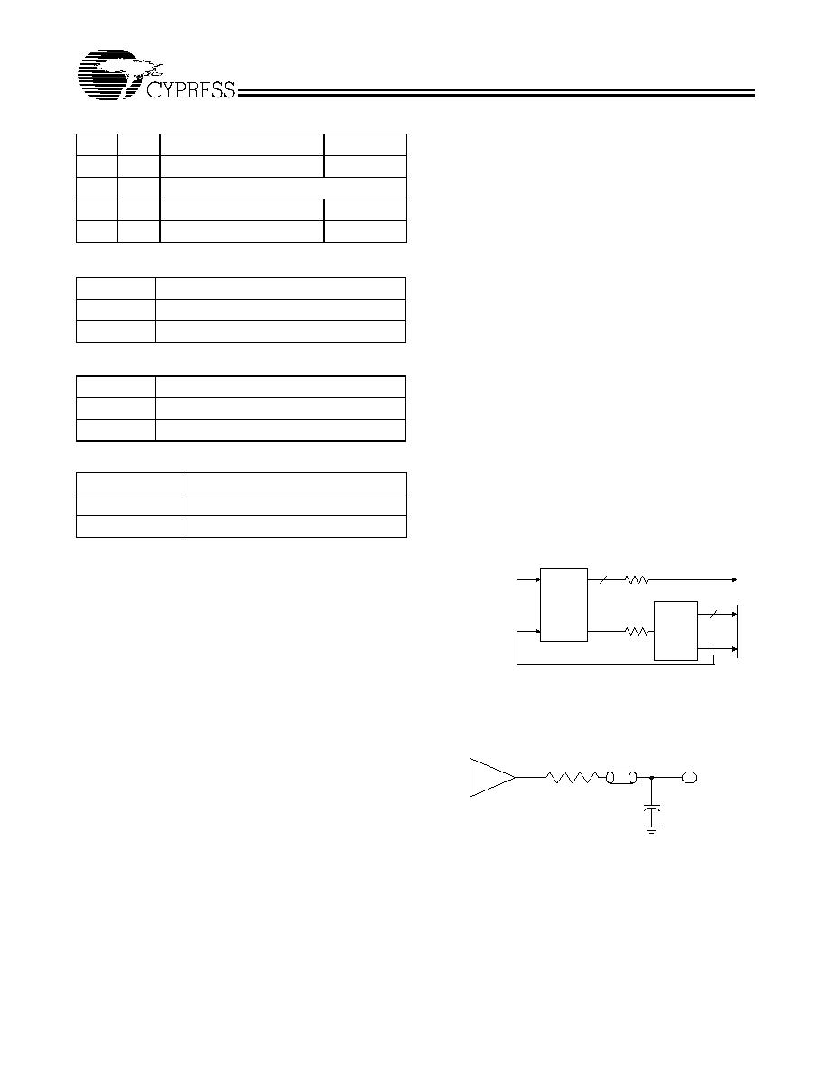
Inserting Other Devices in Feedback Path
Due to the fact that the device has an external feedback path
the user has a wide range of control over its output to input
skewing effect. One of these is to be able to synchronize the
outputs of an external clock that is resultant from any of the
output clocks. This implementation can be applied to any
device (ASIC, multiple output clock buffer/driver, etc.) which is
put into the feedback path.
Referring to Figure 1, if the traces between the ASIC/buffer
and the destination of the clock signal(s) (A) are equal in length
to the trace between the buffer and the FBIN pin (B), the
signals at the destination device(s) (C) will be driven high at
the same time the Reference clock provided to the ZDB goes
high. Synchronizing the other outputs of the ZDB to the outputs
from the ASIC/Buffer is more complex however, as any propa-
gation delay in the ASIC/Buffer must be accounted for.
There are constraints when inserting other devices. If the
devices contain Phase-Locked Loops (PLLs) or excessively
long delay times they can easily cause the overall clocking
system to become unstable as the components interact. For
these designs it is advisable to contact Cypress for applica-
tions support.
Table 1. Output Configuration
S1
S2
Qx source
PLL
0
0
Three-state
Shutdown
0
1
Reserved
1
0
Reference input
Shutdown
1
1
PLL output
Active
Table 2. Frequency Range Setting
Range
Output Frequency Range
0
50≠100 MHz
1
100≠200 MHz
Table 3. Output Configuration Setting
C1
Output Type
0
3.3V Full swing
1
2.5V Full swing
Table 4. Frequency Multiplication Table
MUL
Output Frequency
0
F
OUT
= F
REF
1
F
OUT
= F
REF
x 2
Reference
Signal
Feedback
Input
ASIC/
Buffer
Zero
Delay
Buffer
A
B
C
Figure 1. Output Buffer in the Feedback Path
2 4 O h m
o n c h i p
o u tp u t
b u f f e r
5 p f
4 in c h
5 0 o h m T lin e
Component Characterization Set-up
Figure 2. Termination Networks
CY23020-1
Document #: 38-07120 Rev. *B
Page 4 of 10
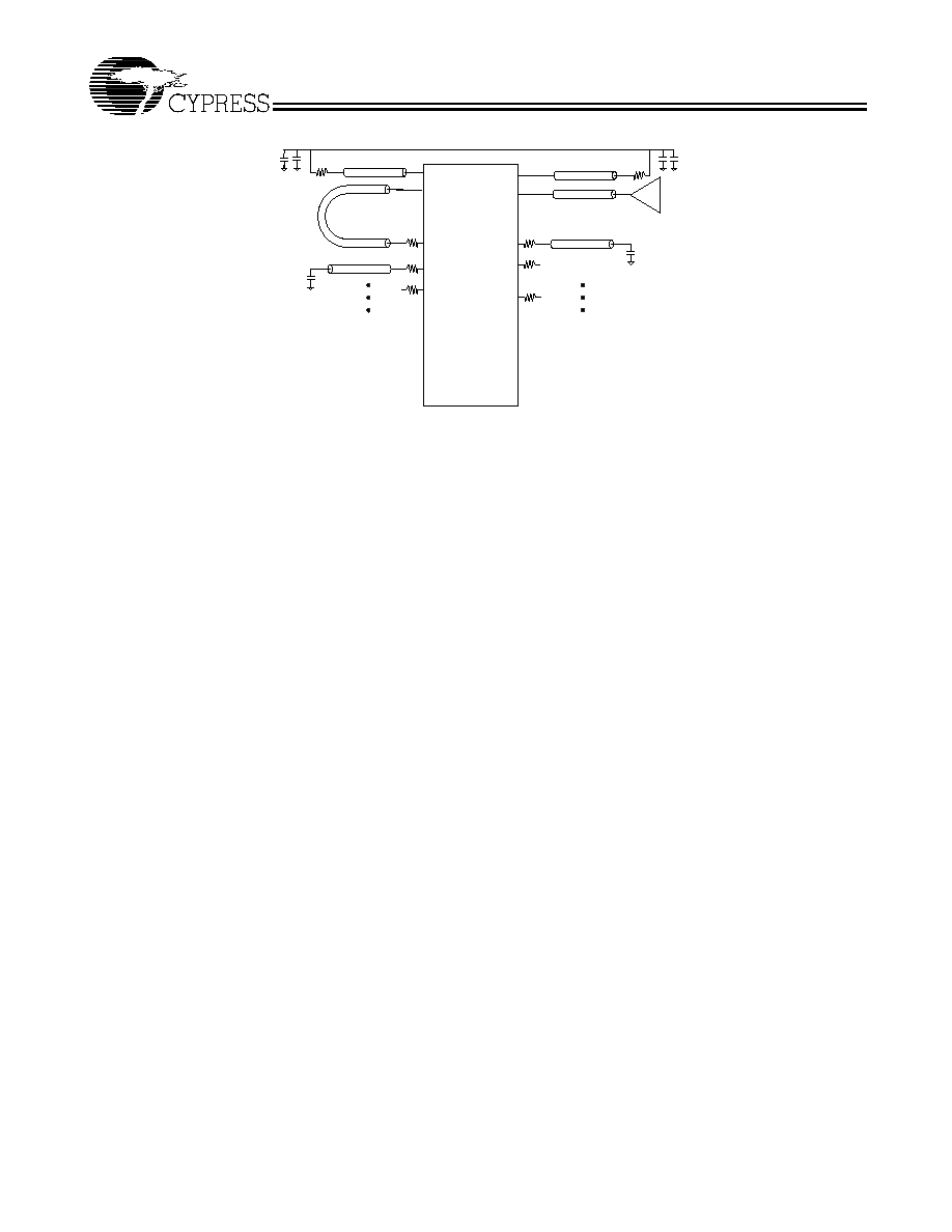
The CY23020-1 uses a differential input receiver to increase
it's rejection of common mode input noise and thus increase
device performance. To ensure that any noise appears equally
on both the REF≠ and REF+ pins, it is necessary to match the
external impedance and circuitry seen at these pins. Figure 3
shows how this may be accomplished. The reference voltage,
V
REF
can be generated by a resistor divider from a power
supply. This potential will adjust the FBIN+ input's triggering
threshold. The reference voltage should be well bypassed so
as to not introduce any single ended noise to the device. Note
that the impedance (50 ohms) is also matched to the FBIN+
line. The 50 ohm resistor is used to create a "like" load on the
REF≠ input clock signal and matches the 50-ohm source
impedance of the REF+ input signal. If the input impedance is
significantly different than 50 ohms, the reference resistor
should be adjusted accordingly.
Ref-
Ref+
FBOUT
Q1
Q19
Q18
Q17
.
.
.
Q10
Q2
.
.
.
Q9
FBIN-
FBIN+
R
S
50
50
Vref Source
C
L
C
L
R
S
C
byp
C
byp
Figure 3. Establishing Reference Voltages

CY23020-1
Document #: 38-07120 Rev. *B
Page 5 of 10
Absolute Maximum Ratings
Stresses greater than those listed in this table may cause
permanent damage to the device. These represent a stress
rating only. Operation of the device at these or any other condi-
tions above those specified in the operating sections of this
specification is not implied. Maximum conditions for extended
periods may affect reliability.
Parameter
Description
Test Conditions
Unit
V
DD
Voltage on any V
DD
pin with respect to GND
≠0.5 to +5.0
V
V
IN
Voltage on any input pin with respect to GND
≠0.5 to V
DD
+ 0.5
V
T
STG
Storage Temperature
≠65 to +150
∞C
T
A
Operation Temperature (TSSOP)
0 to +70
∞C
Operation Temperature (QFN)
≠40 to +85
∞C
T
J
Junction Temperature
+150 max
∞C
P
D
Package Power Dissipation (TSSOP)
1
W
Full Swing DC Electrical Characteristics
V
DDC
= 3.3V ±5%, V
DD
= 2.5V ±5% or 3.3V ±5%
Parameter
Description
Test Conditions
Min.
Typ.
Max.
Unit
V
IH
REF+, FBIN+ Inputs only
2.0
V
V
IL
REF+, FBIN+ Inputs only
0.8
V
V
IH
Logic Inputs only
0.7 ◊ V
DDC
V
V
IL
Logic Inputs only
0.3 ◊ V
DDC
V
I
IH
Output Current in HIGH state V
IN
= V
DD
, (MUL, C1, and RANGE)
100
µ
A
V
IN
= V
DD
, (REF±, FBIN◊, S1, S2)
10
I
IL
Output Current in LOW state VIN = 0V
10
I
PD
Power-down Current
PLL disable mode, S1:S2 = 0
100
µ
A
C
IN
Input Capacitance
5
pF
2.5V Full Swing DC Electrical Characteristics
V
DDC
= 3.3V ±5%, V
DD
= 2.5V ±5%
Parameter
Description
Test Conditions
Min.
Typ.
Max. Unit
I
DD
Supply Current
Unloaded, 200 MHz
225
mA
I
OH
Output Current in HIGH State Measured at pin, no load network, V
OH
= V
DD
≠ 0.35V
≠14
mA
I
OL
Output Current in LOW State Measured at pin, no load network, V
OL
= 0.35V
14
mA
V
REF
External Reference Voltage
Single-ended inputs, see Figure 3
1.19
1.50
V
3.3V Full Swing DC Electrical Characteristics
V
DDC
= 3.3V ±5%, V
DD
= 3.3V ±5%
Parameter
Description
Test Conditions
Min.
Typ.
Max.
Unit
I
DD
Supply Current
Unloaded, 200 MHz
240
mA
I
OH
Output Current in HIGH State measured at pin, no load network, V
OH
= 2.4V
≠18
mA
I
OL
Output Current in LOW State
measured at pin, no load network, V
OL
= 0.4V
14
mA
V
REF
External Reference Voltage
Single-ended inputs, see Figure 3
0.34 ◊ V
DD
0.46 ◊ V
DD
V

CY23020-1
Document #: 38-07120 Rev. *B
Page 6 of 10
Full Swing AC Electrical Characteristics
V
DDC
= 3.3V ±5%, V
DD
= 2.5V ±5% or V
DD
= 3.3V ±5%,
Load: (See term. diagram, C
L
= 5 pF) TSSOP Package
Parameter
Description
Test Conditions
Min.
Typ.
Max.
Unit
F
IN
Input Frequency
50
200
MHz
F
OUT
Output Frequency
50
200
MHz
t
ISR
Input Slew Rate (+ or ≠)
Measured between 20% and 80% of input swing
1
6.5
V/ns
t
R
Output Rise Rate
Measured between 20% and 80% of output swing
1
6.5
V/ns
t
F
Output Fall Rate
Measured between 80% and 20% of output swing
1
6.5
V/ns
t
IDC
Input Duty Cycle
Tested at 50% swing
40
60
%
t
D
Output Duty Cycle
Measured at V
DD
/2, F
OUT
< 167 MHz
45
55
%
Measured at V
DD
/2, F
OUT
>167 MHz
43
57
t
PD
REF≠FBIN skew
F
out
= F
ref
, V
DD
= 2.5V
≠175
175
ps
F
out
= F
ref
, V
DD
= 3.3V
≠175
225
t
PD2
REF≠FBIN skew
F
out
= F
ref
x2, V
DD
= 2.5V
≠175
175
ps
F
out
= F
ref
x2, V
DD
= 3.3V
≠225
225
t
SK
Output-Output Skew
85
ps
t
TB
Total Timing Budget window
[3, 4]
Refin to any output, F
out
= F
ref
335
ps
Refin to any output, F
out
= F
ref
◊ 2
385
ps
t
JC
Peak Cycle-Cycle Jitter (1000
cycles max)
All outputs active, F
out
= F
ref
95
ps
t
JC_RMS
RMS Cycle-Cycle Jitter
All outputs active, F
out
= F
ref
15
ps
t
JP
Period Jitter p-p
All outputs active, F
out
= F
ref
95
ps
t
JP_RMS
RMS Period Jitter
All outputs active, F
out
= F
ref
15
ps
t
JL
I/O Phase Jitter p-p
All outputs active, F
out
= F
ref
150
ps
t
JLRMS
RMS I/O Phase Jitter
All outputs active, F
out
= F
ref
30
ps
t
JC2
Peak Cycle-Cycle Jitter (1000
cycles max)
All outputs active, F
out
= F
ref
◊ 2
145
ps
t
JCRMS2
RMS Cycle-Cycle Jitter
All outputs active, F
out
= F
ref
◊ 2
25
ps
t
JP2
Period Jitter p-p
All outputs active, F
out
= F
ref
◊ 2
150
ps
t
JPRMS2
RMS Period Jitter
All outputs active, F
out
= F
ref
◊ 2
40
ps
t
JL2
I/O Phase Jitter p-p
All outputs active, F
out
= F
ref
◊ 2
150
ps
t
JLRMS2
RMS I/O Phase Jitter
All outputs active, F
out
= F
ref
◊ 2
30
ps
PSRR
(Core)
I/O Phase Jitter Sensitivity to
Power Supply Variations
1V
pp
modulation of 10 kHz≠10MHz
300
ps
pp
/ V
PSRR
(Output)
I/O Phase Jitter Sensitivity to
Power Supply Variations
1V
pp
modulation of 10 kHz≠10MHz
700
ps
pp
/ V
t
LOCK
Power-up lock time
1
ms
t
PWD
Power-down time
1
ms
t
TSK
Spread Spectrum Tracking skew
100
ps
Notes:
3.
MAX(T
PD_MAX
≠ T
PD_MIN
, T
PD_MAX
,(≠1)*T
PD_MIN
) where T
PD _MAX
is the longest delay of refin to any output measured over at least 1000 cycles and T
PD
_
MIN
is the minimum (may be negative) delay observed over all outputs over at least 1000 cycles.
4.
Guaranteed by statistical correlation. Tested initially and after any design or process changes that may affect this parameter.

CY23020-1
Document #: 38-07120 Rev. *B
Page 7 of 10
Full Swing AC Electrical Characteristics
V
DDC
=3.3V ±5%, V
DD
= 2.5V ±5% or V
DD
= 3.3V ±5%,
Load: (See term. diagram, C
L
= 5 pf) QFN Package
Parameter
Description
Test Conditions
Min.
Typ.
Max.
Unit
F
IN
Input Frequency
50
200
MHz
F
OUT
Output Frequency
50
200
MHz
t
ISR
Input Slew Rate (+ or ≠)
Measured between 20% and 80% of input swing
1
6.5
V/ns
t
R
Output Rise Rate
Measured between 20% and 80% of output swing
1
6.5
V/ns
t
F
Output Fall Rate
Measured between 80% and 20% of output swing
1
6.5
V/ns
t
IDC
Input Duty Cycle
Tested at 50% swing
40
60
%
t
D
Output Duty Cycle
Measured at V
DD
/2
45
55
%
t
PD
REF≠FBIN skew
F
out
= F
ref
, V
DD
= 2.5V
≠175
175
ps
F
out
= F
ref
, V
DD
= 3.3V
≠100
175
t
PD2
REF≠FBIN skew
F
out
= F
ref
x2, V
DD
= 2.5V
≠175
175
ps
F
out
= F
ref
x2, V
DD
= 3.3V
≠150
175
t
SK
Output-Output Skew
85
ps
t
TB
Total Timing Budget window
[3,4]
Refin to any output, F
out
= F
ref
335
ps
All outputs active, F
out
= F
ref
◊ 2
385
ps
t
JC
Peak Cycle-Cycle Jitter (1000
cycles max)
All outputs active, F
out
= F
ref
95
ps
t
JC_RMS
RMS Cycle-Cycle Jitter
All outputs active, F
out
= F
ref
12
ps
t
JP
Period Jitter p-p
All outputs active, F
out
= F
ref
95
ps
t
JP_RMS
RMS Period Jitter
All outputs active, F
out
= F
ref
17
ps
t
JL
I/O Phase Jitter p-p
All outputs active, F
out
= F
ref
170
ps
t
JLRMS
RMS I/O Phase Jitter
All outputs active, F
out
= F
ref
22
ps
t
JC2
Peak Cycle-Cycle Jitter (1000
cycles max)
All outputs active, F
out
= F
ref
◊ 2
145
ps
t
JCRMS2
RMS Cycle-Cycle Jitter
All outputs active, F
out
= F
ref
◊ 2
24
ps
t
JP2
Period Jitter p-p
All outputs active, F
out
= F
ref
◊ 2
170
ps
t
JPRMS2
RMS Period Jitter
All outputs active, F
out
= F
ref
◊ 2
28
ps
t
JL2
I/O Phase Jitter p-p
All outputs active, F
out
= F
ref
◊ 2
170
ps
t
JLRMS2
RMS I/O Phase Jitter
All outputs active, F
out
= F
ref
◊ 2
28
ps
PSRR
(Core)
I/O Phase Jitter Sensitivity to
Power Supply Variations
1V
pp
modulation of 10 kHz≠10MHz
300
ps
pp
/ V
PSRR
(Output)
I/O Phase Jitter Sensitivity to
Power Supply Variations
1V
pp
modulation of 10 kHz≠10MHz
700
ps
pp
/ V
t
LOCK
Power-up lock time
1
ms
t
PWD
Power-down time
1
ms
t
TSK
Spread Spectrum Tracking
skew
100
ps

CY23020-1
Document #: 38-07120 Rev. *B
Page 8 of 10
Package Diagrams
Note:
5.
Theta J = 95∞ C/W for TSSOP package.
Ordering Information
Base Part #
Package
Temperature Range
CY23020ZC≠1
48-pin TSSOP
[5]
Commercial, 0∞C to +70∞C
CY23020ZC≠1T
48-pin TSSOP--Tape and Reel
Commercial, 0∞C to +70∞C
CY23020LFI≠1
48- pin QFN
Industrial, ≠40∞C to +85∞C
CY23020LFI≠1T
48-pin QFN--Tape and Reel
Industrial, ≠40∞C to +85∞C
48-Lead Thin Shrunk Small Outline Package, Type II (6 mm ◊ 12 mm) Z48
51-85059-B

CY23020-1
Document #: 38-07120 Rev. *B
Page 9 of 10
© Cypress Semiconductor Corporation, 2002. The information contained herein is subject to change without notice. Cypress Semiconductor Corporation assumes no responsibility for the use
of any circuitry other than circuitry embodied in a Cypress Semiconductor product. Nor does it convey or imply any license under patent or other rights. Cypress Semiconductor does not authorize
its products for use as critical components in life-support systems where a malfunction or failure may reasonably be expected to result in significant injury to the user. The inclusion of Cypress
Semiconductor products in life-support systems application implies that the manufacturer assumes all risk of such use and in doing so indemnifies Cypress Semiconductor against all charges.
Package Diagrams
(continued)
Spread Aware, Total Timing Budget, and TTB are trademarks of Cypress Semiconductor. All product and company names
mentioned in this document are the trademarks of their respective holders.
48-Lead QFN (7x7 mm) LF48
51-85152-*A

CY23020-1
Document #: 38-07120 Rev. *B
Page 10 of 10
Document Title: CY23020-1 20-output, 200-MHz Zero Delay Buffer
Document Number: 38-07120
REV.
ECN No.
Issue Date
Orig. of
Change
Description of Change
**
109287
10/30/01
SZV
New Data Sheet
*A
113758
07/22/02
CTK
Updated to reflect latest characteristics data
*B
118945
11/06/02
HWT
Added the QFN Package in this device