MediaClockTM
MPEG Clock Generator with VCXO
CY24212
PRELIMINARY
Cypress Semiconductor Corporation
∑
3901 North First Street
∑
San Jose, CA 95134
∑
408-943-2600
Document #: 38-07402 Rev. *B
Revised February 18, 2003
Features
Benefits
∑ Integrated phase-locked loop (PLL)
Highest-performance PLL tailored for multimedia applications
∑ Low jitter, high-accuracy outputs
Meets critical timing requirements in complex system designs
∑ VCXO with analog adjust
Large ±150-ppm range, better linearity
∑ 3.3V operation
Enables application compatibility
Part Number
Outputs
Input Frequency Range
Output Frequencies
CY24212-1
1
13.5 MHz/27 MHz (selectable)
27 MHz
CY24212-2
2
13.5 MHz/27 MHz (selectable)
Two copies of 27 MHz
CY24212-3
2
27 MHz
27 MHz/27.027 MHz (-1 ppm)
CY24212-5
2
27 MHz
27 MHz/27.027 MHz (0 ppm)
Table 1. CY24212 (-1, -2) Frequency Select Option
FSEL
Reference
CLKA/CLKB
0
13.5 MHz
27 MHz
1
27 MHz
27 MHz
Table 2. CY24212 (-3, -5) Frequency Select Option
FSEL
Reference
CLKA
CLKB
0
27 MHz
27 MHz
27 MHz
1
27 MHz
27 MHz
27.027 MHz
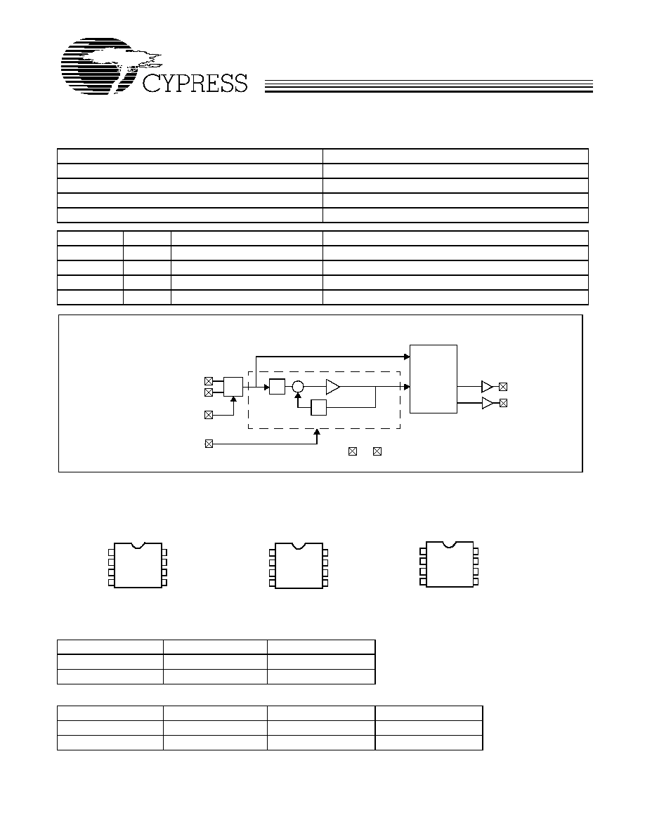
Logic Block Diagram
XOUT
OUTPUT
DIVIDERS
PLL
OSC
VCXO
Q
P
VCO
VDD
VSS
CLKA (27 MHz)
XIN
FSEL
27 MHz (-2)
27/27.027 MHz (-3)
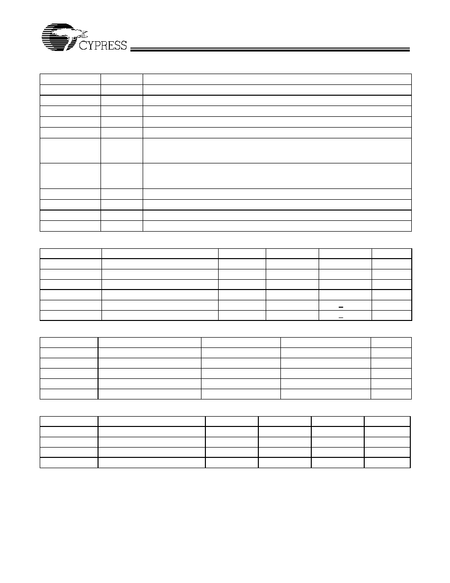
8-pin SOIC
CY24212-1
Pin Configurations
1
2
3
4
XOUT
XIN
VCXO
CLKA 27 MHz
VSS
VSS
FSEL
5
6
7
8
VDD
8-pin SOIC
CY24212-2
1
2
3
4
XOUT
XIN
VCXO
CLKA 27 MHz
VSS
CLKB 27 MHz
FSEL
5
6
7
8
VDD
8-pin SOIC
CY24212-3,-5
1
2
3
4
XOUT
XIN
VCXO
CLKA 27 MHz
VSS
CLKB (27/27.027 MHz)
FSEL
5
6
7
8
VDD
CY24212
PRELIMINARY
Document #: 38-07402 Rev. *B
Page 2 of 6
Pin Description
Name
Pin Number Description
XIN
1
Reference Input.
VDD
2
Voltage Supply.
VCXO
3
Input Analog Control for VCXO.
VSS
4
Ground.
CLKA
5
27-MHz Clock Output.
FSEL (-1,-2)
6
Input Frequency Select, Weak Internal Pull-up.
FSEL = 0, XIN = 13.5 MHz
FSEL = 1, XIN = 27 MHz
FSEL (-3,-5)
6
Output Frequency Select, Weak Internal Pull-up.
FSEL = 0, CLKA = 27 MHz, CLKB = 27 MHz
FSEL = 1, CLKA = 27 MHz, CLKB = 27.027 MHz
VSS (-1)
7
Ground.
CLKB (-2)
7
27 MHz.
CLKB (-3,-5)
7
27 MHz/27.027 MHz.
XOUT
[1]
8
Reference Output.
Pullable Crystal Specifications
Parameter
Name
Min
Typ
Max
Unit
CR
load
Crystal Load Capacitance
14
pF
C0/C1
240
ESR
Equivalent Series Resistance
35
50
T
o
Operating Temperature
0
70
∞C
Crystal Accuracy
Crystal Accuracy
+ 20
ppm
TT
s
Stability over Temperature and Aging
+ 50
ppm
Absolute Maximum Conditions
Parameter
Description
Min
Max
Unit
V
DD
Supply Voltage
≠0.5
7.0
V
T
S
Storage Temperature
[2]
≠65
125
∞C
T
J
Junction Temperature
125
∞C
Digital Inputs
V
SS
≠ 0.3
V
DD
+ 0.3
V
Electrostatic Discharge
2
kV
Recommended Operating Conditions
Parameter
Description
Min
Typ
Max
Unit
V
DD
Operating Voltage
3.135
3.3
3.465
V
T
A
Ambient Temperature
0
70
∞C
C
LOAD
Max. Load Capacitance
15
pF
f
REF
Reference Frequency
13.5
27
MHz
Notes:
1.
Float XOUT if XIN is externally driven.
2.
Rated for ten years.
CY24212
PRELIMINARY
Document #: 38-07402 Rev. *B
Page 3 of 6
DC Electrical Specifications
Parameter
Name
Description
Min
Typ
Max
Unit
I
OH
Output High Current
V
OH
= V
DD
≠ 0.5, V
DD
= 3.3V (source)
12
24
mA
I
OL
Output Low Current
V
OL
= 0.5, V
DD
= 3.3V (sink)
12
24
mA
C
IN
Input Capacitance
7
pF
I
IH
Input High Current
V
IH
= V
DD
≠
5
10
µ
A
I
IL
Input Low Current
V
IL
= 0V
≠
≠
50
µ
A
f
XO
VCXO Pullability Range
+150
ppm
V
VCXO
VCXO Input Range
0
V
DD
V
I
DD
Supply Current
Sum of Core and Output Current
35
mA
V
IH
Input High Voltage
CMOS levels, 70% of V
DD
0.7
V
DD
V
IL
Input Low Voltage
CMOS levels, 30% of V
DD
0.3
V
DD
R
UP
Pull-up resistor on inputs
V
DD
= 3.14 to 3.47V, measured V
IN
= 0V
100
150
k
AC Electrical Specifications (V
DD
= 3.3V)
Parameter
[3]
Name
Description
Min
Typ
Max
Unit
DC
Output Duty Cycle
Duty Cycle is defined in Figure 1, 50% of V
DD
45
50
55
%
ER
Rising Edge Rate
Output Clock Edge Rate, Measured from 20%
to 80% of V
DD
, C
LOAD
= 15 pF. See Figure 2.
0.8
1.4
V/ns
EF
Falling Edge Rate
Output Clock Edge Rate, Measured from 80%
to 20% of V
DD
, C
LOAD
= 15 pF. See Figure 2.
0.8
1.4
V/ns
t
9
Clock Jitter
Peak-to-peak period jitter
300
ps
t
10
PLL Lock Time
3
ms
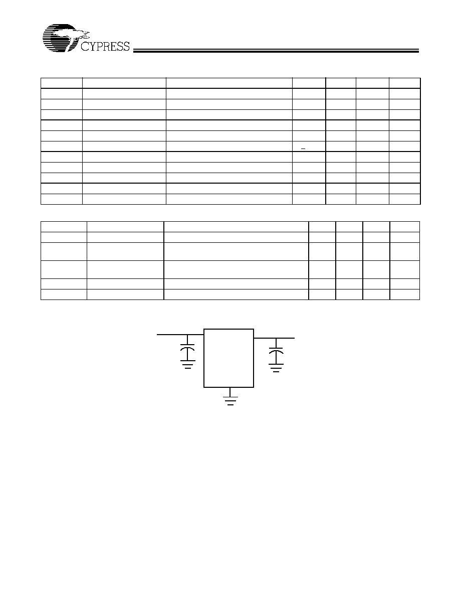
Test and Measurement Set-up
Note:
3.
Not 100% tested.
0.1
µ
F
V
DDs
Outputs
C
LOAD
GND
DUT
CY24212
PRELIMINARY
Document #: 38-07402 Rev. *B
Page 4 of 6
Voltage and Timing Definitions
Ordering Information
Ordering Code
Package Name
Package Type
Operating Range
Operating Voltage
CY24212SC-1
S8
8-Pin SOIC
Commercial
3.3V
CY24212SC-1T
S8
8-Pin SOIC -Tape and Reel
Commercial
3.3V
CY24212SC-2
S8
8-Pin SOIC
Commercial
3.3V
CY24212SC-2T
S8
8-Pin SOIC -Tape and Reel
Commercial
3.3V
CY24212SC-3
S8
8-Pin SOIC
Commercial
3.3V
CY24212SC-3T
S8
8-Pin SOIC -Tape and Reel
Commercial
3.3V
CY24212SC-5
S8
8-Pin SOIC
Commercial
3.3V
CY24212SC-5T
S8
8-Pin SOIC -Tape and Reel
Commercial
3.3V
Clock
Output
V
DD
50% of V
DD
0V
t
1
t
2
Figure 1. Duty Cycle Definition
Clock
Output
t
3
t
4
V
DD
80% of V
DD
20% of V
DD
0V
Figure 2. ER = (0.6 x V
DD
) /t3, EF = (0.6 x V
DD
) /t4
CY24212
PRELIMINARY
Document #: 38-07402 Rev. *B
Page 5 of 6
© Cypress Semiconductor Corporation, 2003. The information contained herein is subject to change without notice. Cypress Semiconductor Corporation assumes no responsibility for the use
of any circuitry other than circuitry embodied in a Cypress Semiconductor product. Nor does it convey or imply any license under patent or other rights. Cypress Semiconductor does not authorize
its products for use as critical components in life-support systems where a malfunction or failure may reasonably be expected to result in significant injury to the user. The inclusion of Cypress
Semiconductor products in life-support systems application implies that the manufacturer assumes all risk of such use and in doing so indemnifies Cypress Semiconductor against all charges.
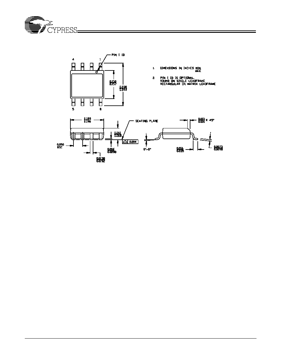
Package Drawing and Dimensions
MediaClock is a trademark of Cypress Semiconductor Corporation. All product and company names mentioned in this document
may be the trademarks of their respective holders.
8-Lead (150-Mil) SOIC S8
51-85066-*A
CY24212
PRELIMINARY
Document #: 38-07402 Rev. *B
Page 6 of 6
Document History Page
Document Title: CY24212 MediaClockTM MPEG Clock Generator with VCXO
Document Number: 38-07402
REV.
ECN NO.
Issue
Date
Orig. of
Change
Description of Change
**
117089
09/09/02
CKN
New Data Sheet
*A
120888
12/06/02
CKN
Added -3
*B
123064
02/19/03
CKN
Added -5