Frequency Generator for Intel
Æ
Integrated Chipset
CY28301
Cypress Semiconductor Corporation
∑
3901 North First Street
∑
San Jose
∑
CA 95134
∑
408-943-2600
Document #: 38-07011 Rev. *C
Revised September 24, 2002
Features
∑ Single chip FTG solution for Intel
Æ
Solano/810E/810
∑ Support SMBus byte Read/Write and block Read/Write
operations to simplify system BIOS development
∑ Vendor ID and revision ID support
∑ Maximized EMI suppression using Cypress's Spread
Spectrum technology
∑ Low jitter and tightly controlled clock skew
∑ Two copies of CPU clock
∑ Thirteen copies of SDRAM clock
∑ Eight copies of PCI clock
∑ One copy of synchronous APIC clock
∑ Three copies of 66-MHz outputs
∑ Two copies of 48-MHz outputs
∑ One copy of 14.31818-MHz reference clock
Key Specifications
CPU, SDRAM Outputs Cycle-to-Cycle Jitter: ............. 250 ps
APIC, 48-MHz, 3V66, PCI Outputs
Cycle-to-Cycle Jitter: ................................................... 500 ps
CPU, 3V66 Output Skew: ............................................ 175 ps
SDRAM, APIC, 48-MHz Output Skew: ........................ 250 ps
PCI Output Skew: ........................................................ 500 ps
CPU to SDRAM Skew (@ 133 MHz) ......................... ±0.5 ns
CPU to SDRAM Skew (@ 100 MHz).................. 4.5 to 5.5 ns
CPU to 3V66 Skew (@ 66 MHz) ........................ 7.0 to 8.0 ns
3V66 to PCI Skew (3V66 lead)........................... 1.5 to 3.5 ns
PCI to APIC Skew ...................................................... ±0.5 ns
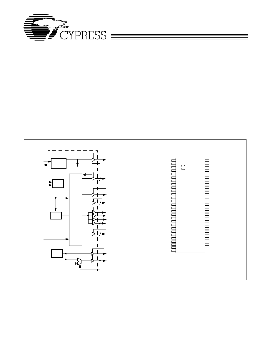
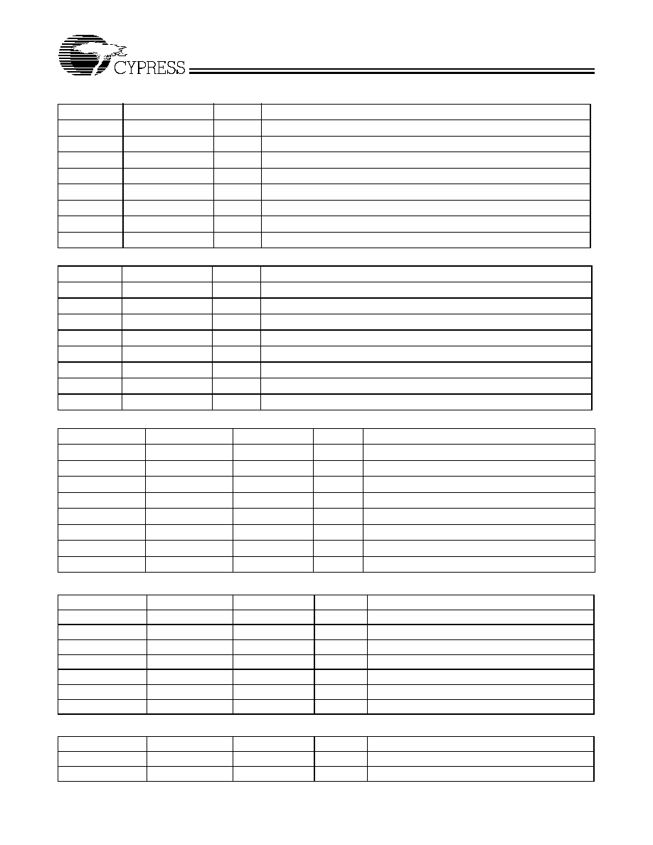
VDD_REF
VDD_CPU
PCI1
XTAL
PLL REF FREQ
PLL 1
X2
X1
REF/FS1
PCI3:7
48MHz/FS0
24_48MHz
PLL2
OSC
VDD_48MHz
SMBus
SDATA
Logic
SCLK
3V66_0:2
CPU0:1
APIC
Divider,
Delay, and
Phase
Control
Logic
3
VDD_3V66
2
SDRAM0:11,
13
PCI0
PCI2/SEL24_48MHz#*
/2
(FS0:4)
5
VDD_REF
X1
X2
GND_REF
GND_3V66
3V66_0
3V66_1
3V66_2
VDD_3V66
VDD_PCI
PCI0
PCI1
PCI2/SEL24_48MHz#*
GND_PCI
PCI3
PCI4
PCI5
VDD_PCI
PCI6
PCI7
GND_PCI
PD#*
SCLK
SDATA
CY
283
01
REF/FS1*
VDD_APIC
APIC
VDD_CPU
CPU0
CPU1
GND_CPU
GND_SDRAM
SDRAM0
SDRAM1
SDRAM2
VDD_SDRAM
SDRAM3
SDRAM4
SDRAM5
GND_SDRAM
SDRAM6
SDRAM7
SDRAM_F
VDD_SDRAM
GND_48MHz
24_48MHz
48MHz/FS0*
VDD_48MHz
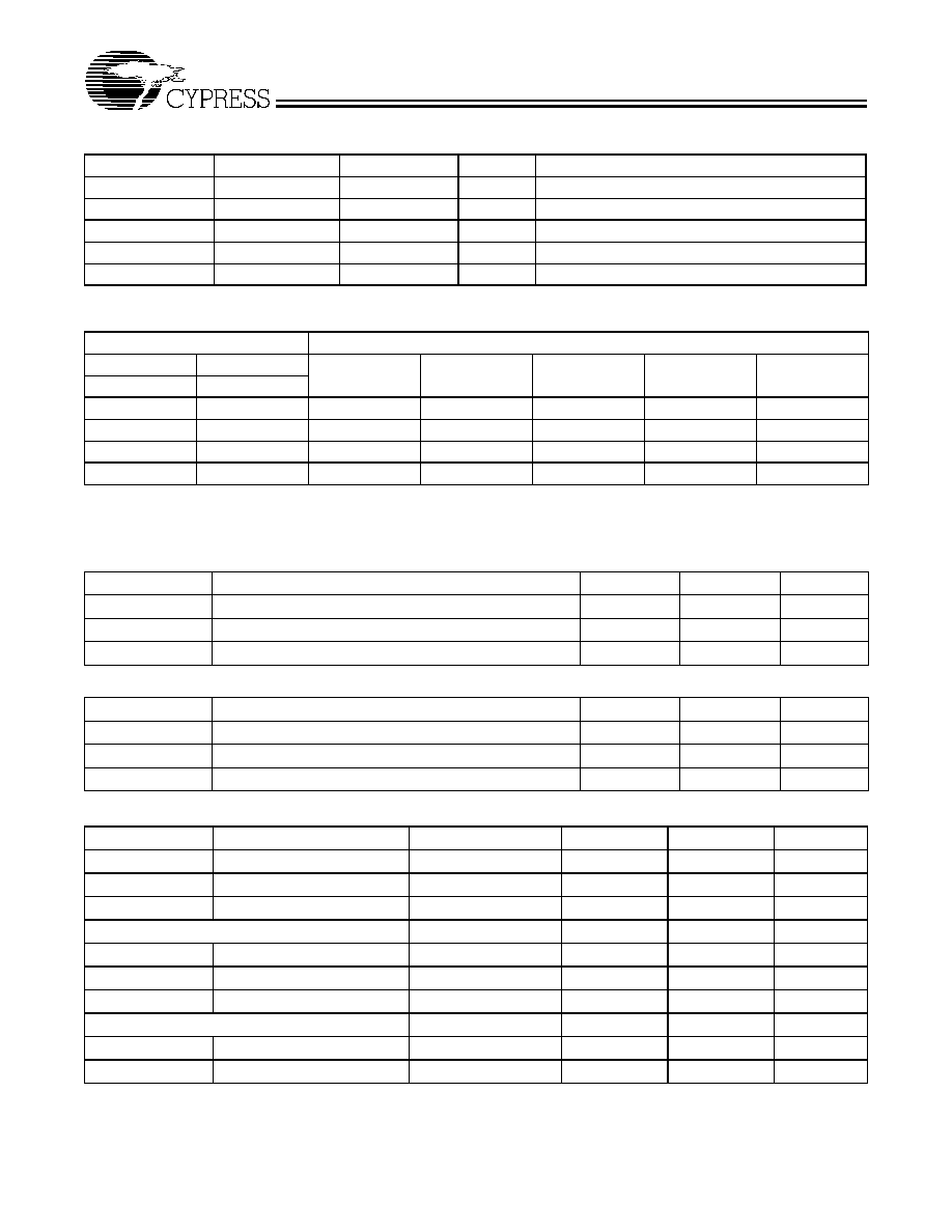
56
55
54
53
52
51
50
49
48
47
46
45
44
43
42
41
40
39
38
37
36
35
34
33
1
2
3
4
5
6
7
8
9
10
11
12
13
14
15
16
17
18
19
20
21
22
23
24
25
26
27
28
32
31
30
29
VDD_SDRAM
SDRAM11
SDRAM10
GND_SDRAM
VDD_SDRAM
SDRAM8
SDRAM9
GND_SDRAM
VDD_APIC
SDRAM_F
VDD_SDRAM
VDD_PCI
PD#
Note:
1.
Internal 100K pull-up resistors present on inputs marked with *. Design
should not rely solely on internal pull-up resistor to set I/O pins HIGH.
Pin Configuration
[1]
Block Diagram
CY28301
Document #: 38-07011 Rev. *C
Page 2 of 15
Pin Definitions
Pin Name
Pin No.
Pin
Type
Pin Description
REF/FS1
56
I/O
Reference Clock /Frequency Select 1: 3.3V 14.318-MHz clock output.
This pin also serves as the select strap to determine the device operating
frequency (as described in Table 5).
X1
2
I
Crystal Input: This pin has dual functions. It can be used as an external
14.318-MHz crystal connection or as an external reference frequency
input.
X2
3
O
Crystal Output: An input connection for an external 14.318-MHz crystal
connection. If using an external reference, this pin must be left
unconnected.
PCI0
11
O
PCI Clock 0: 3.3V 33-MHz PCI clock output.
PCI1
12
O
PCI Clock 1: 3.3V 33-MHz PCI clock output.
PCI2/SEL24_48MHz#
13
O
PCI Clock 2/Select 24 or 48 MHz: 3.3V 33-MHz PCI clock outputs. This
pin also serves as the select strap to determine the output frequency for
24_48MHz output. Logic 1 = 24 MHz on pin 35.
PCI3:7
15, 16, 17, 19,
20
O
PCI Clock 3 through 7: 3.3V 33-MHz PCI clock outputs. PCI0:7 can be
individually turned off via the SMBus interface.
3V66_0:2
6, 7, 8
O
66-MHz Clock Output: 3.3V output clocks. The operating frequency is
controlled by FS0:1 (see Table 5).
48MHz/FS0
34
I/O
48-MHz Output/Frequency Selection 1: 3.3V 48-MHz non-spread
spectrum output. This pin also serves as the select strap to determine the
device operating frequency (as described in Table 5.)
24_48MHz
35
O
24- or 48-MHz Output: 3.3V 24- or 48-MHz non-spread spectrum output.
PD#
22
I
Power-down Input: LVTTL-compatible asynchronous input that places
the device in power-down mode when held LOW.
CPU0:1
52, 51
O
CPU Clock Outputs: Clock outputs for the host bus interface. Output
frequencies depending on the configuration of FS0:1. Voltage swing is set
by VDDQ2.
SDRAM0:11,
SDRAM_F
48, 47, 46, 44,
43, 42, 40, 39,
31, 30, 27, 26,
38
O
SDRAM Clock Outputs: 3.3V outputs for SDRAM and chipset. The
operating frequency is controlled by FS0:1 (see Table 5).
APIC
54
O
Synchronous APIC Clock Outputs: Clock outputs running synchronous
with the PCI clock outputs. Voltage swing set by VDDQ2.
SDATA
24
I/O
Data pin for SMBus circuitry.
SCLK
23
I
Clock pin for SMBus circuitry.
VDD_REF,
VDD_3V66, VDD_PCI,
VDD_SDRAM,
VDD_48MHz
1, 9, 10, 18, 25,
32, 37, 45, 33
P
3.3V Power Connection: Power supply for SDRAM output buffers, PCI
output buffers, reference output buffers, and 48-MHz output buffers.
Connect to 3.3V.
VDD_CPU,
VDD_APIC
53, 55
P
2.5V Power Connection: Power supply for APIC and CPU output buffers.
Connect to 2.5V.
GND_REF,
GND_3V66,
GND_PCI,
GND_SDRAM,
GND_48MHZ,
GND_CPU
4, 5, 14, 21, 28,
29, 41, 49, 50,
36
G
Ground Connections: Connect all ground pins to the common system
ground plane.
CY28301
Document #: 38-07011 Rev. *C
Page 3 of 15
Serial Data Interface
The CY28301 features a two-pin, serial data interface that can
be used to configure internal register settings that control
particular device functions.
Data Protocol
The clock driver serial protocol supports byte/word Write,
byte/word Read, block Write, and block Read operations from
the controller. For block Write/Read operation, the bytes must
be accessed in sequential order from lowest to highest byte
with the ability to stop after any complete byte has been trans-
ferred. For byte/word Write and byte Read operations, the
system controller can access individual indexed bytes. The
offset of the indexed byte is encoded in the command code.
The definition for the command code is defined as follows.
Table 1. Command Code Definition
Bit
Descriptions
7
0 = Block Read or block Write operation
1 = Byte/Word Read or byte/word Write operation
6:0
Byte offset for byte/word Read or Write operation. For block Read or Write operations, these
bits need to be set at `0000000.'
Table 2. Block Read and Block Write Protocol
Block Write Protocol
Block Read Protocol
Bit
Description
Bit
Description
1
Start
1
Start
2:8
Slave address ≠ 7 bits
2:8
Slave address ≠ 7 bits
9
Write
9
Write
10
Acknowledge from slave
10
Acknowledge from slave
11:18
Command code ≠ 8-bits
`00000000' stands for block operation
11:18
Command code ≠ 8 bits
`00000000' stands for block operation
19
Acknowledge from slave
19
Acknowledge from slave
20:27
Byte count ≠ 8 bits
20
Repeat start
28
Acknowledge from slave
21:27
Slave address ≠ 7 bits
29:36
Data byte 0 ≠ 8 bits
28
Read
37
Acknowledge from slave
29
Acknowledge from slave
38:45
Data byte 1 ≠ 8 bits
30:37
Byte count from slave ≠8 bits
46
Acknowledge from slave
38
Acknowledge
...
Data byte N/Slave acknowledge...
39:46
Data byte from slave ≠ 8 bits
...
Data byte N ≠ 8 bits
47
Acknowledge
...
Acknowledge from slave
48:55
Data byte from slave ≠ 8 bits
...
Stop
56
Acknowledge
...
Data bytes from slave/acknowledge
...
Data byte N from slave ≠ 8 bits
...
Not acknowledge
...
Stop
CY28301
Document #: 38-07011 Rev. *C
Page 4 of 15
Table 3. Word Read and Word Write Protocol
Word Write Protocol
Word Read Protocol
Bit
Description
Bit
Description
1
Start
1
Start
2:8
Slave address ≠ 7 bits
2:8
Slave address ≠ 7 bits
9
Write
9
Write
10
Acknowledge from slave
10
Acknowledge from slave
11:18
Command Code ≠ 8-bits
`1xxxxxxx' stands for byte or word operation
bit[6:0] of the command code represents the
offset of the byte to be accessed
11:18
Command code ≠ 8 bits
`1xxxxxxx' stands for byte or word operation
bit[6:0] of the command code represents the
offset of the byte to be accessed
19
Acknowledge from slave
19
Acknowledge from slave
20:27
Data byte low ≠ 8 bits
20
Repeat start
28
Acknowledge from slave
21:27
Slave address ≠ 7 bits
29:36
Data byte high ≠ 8 bits
28
Read
37
Acknowledge from slave
29
Acknowledge from slave
38
Stop
30:37
Data byte low from slave ≠ 8 bits
38
Acknowledge
39:46
Data byte high from slave ≠ 8 bits
47
Not acknowledge
48
Stop
Table 4. Byte Read and Byte Write Protocol
Byte Write Protocol
Byte Read Protocol
Bit
Description
Bit
Description
1
Start
1
Start
2:8
Slave address ≠ 7 bits
2:8
Slave address ≠ 7 bits
9
Write
9
Write
10
Acknowledge from slave
10
Acknowledge from slave
11:18
Command code 8 ≠ bits
`1xxxxxxx' stands for byte operation
bit[6:0] of the command code represents the
offset of the byte to be accessed
11:18
Command code ≠ 8 bits
`1xxxxxxx' stands for byte operation
bit[6:0] of the command code represents the
offset of the byte to be accessed
19
Acknowledge from slave
19
Acknowledge from slave
20:27
Data byte 8 ≠ bits
20
Repeat start
28
Acknowledge from slave
21:27
Slave address ≠ 7 bits
29
Stop
28
Read
29
Acknowledge from slave
30:37
Data byte from slave ≠ 8 bits
38
Not Acknowledge
39
Stop
CY28301
Document #: 38-07011 Rev. *C
Page 5 of 15
CY28301 Serial Configuration Map
1. The serial bits will be read by the clock driver in the following
order:
Byte 0 ≠ Bits 7, 6, 5, 4, 3, 2, 1, 0
Byte 1 ≠ Bits 7, 6, 5, 4, 3, 2, 1, 0
Byte N ≠ Bits 7, 6, 5, 4, 3, 2, 1, 0
2. All unused register bits (reserved and N/A) should be
written to a "0" level.
3. All register bits labeled "Initialize to 0" must be written to "0"
during initialization.
Byte 0: Control Register 0
Bit
Pin#
Name
Default
Description
Bit 7
≠
SEL1
0
See 5
Bit 6
≠
SEL0
0
See 5
Bit 5
≠
Reserved
0
Reserved
Bit 4
≠
Reserved
0
Reserved
Bit 3
≠
FS_Override
0
0 = Select operating frequency by FS[1:0] input pins
1 = Select operating frequency by SEL[1:0] settings
Bit 2
≠
Spread Select2
0
`000' = Normal (spread off)
`001' = Test mode
`010' = Reserved
`011' = Three-stated
`100' = ≠0.5%
`101' = ≠0.75%
`110' = ≠1.0%
`111' = ≠0.3%
Bit 1
≠
Spread Select1
0
Bit 0
≠
Spread Select0
0
Byte 1: Control Register 1
Bit
Pin#
Name
Default
Description
Bit 7
56
Latched FS1 input
X
Latched FS[1:0] inputs. These bits are Read-only.
Bit 6
34
Latched FS0 input
X
Bit 5
≠
Reserved
0
Reserved
Bit 4
≠
Reserved
0
Reserved
Bit 3
≠
Reserved
0
Reserved
Bit 2
≠
Reserved
0
Reserved
Bit 1
56
REF
1
(Active/Inactive)
Bit 0
56
REF_DRV
0
REF Clock output drive strength
0 = Normal
1= High drive
CY28301
Document #: 38-07011 Rev. *C
Page 6 of 15
Byte 2: Control Register 2
Bit
Pin#
Name
Default
Description
Bit 7
20
PCI7
1
(Active/Inactive)
Bit 6
19
PCI6
1
(Active/Inactive)
Bit 5
17
PCI5
1
(Active/Inactive)
Bit 4
16
PCI4
1
(Active/Inactive)
Bit 3
15
PCI3
1
(Active/Inactive)
Bit 2
13
PCI2
1
(Active/Inactive)
Bit 1
12
PCI1
1
(Active/Inactive)
Bit 0
11
PCI0
1
(Active/Inactive)
Byte 3: Control Register 3
Bit
Pin#
Name
Default
Description
Bit 7
8
3V66_2
1
(Active/Inactive)
Bit 6
7
3V66_1
1
(Active/Inactive)
Bit 5
6
3V66_0
1
(Active/Inactive)
Bit 4
54
APIC
1
(Active/Inactive)
Bit 3
≠
Reserved
0
Reserved
Bit 2
≠
Reserved
0
Reserved
Bit 1
51
CPU1
1
(Active/Inactive)
Bit 0
52
CPU0
1
(Active/Inactive)
Byte 4: Control Register 4
Bit
Pin#
Name
Default
Description
Bit 7
39
SDRAM7
1
(Active/Inactive)
Bit 6
40
SDRAM6
1
(Active/Inactive)
Bit 5
42
SDRAM5
1
(Active/Inactive)
Bit 4
43
SDRAM4
1
(Active/Inactive)
Bit 3
44
SDRAM3
1
(Active/Inactive)
Bit 2
46
SDRAM2
1
(Active/Inactive)
Bit 1
47
SDRAM1
1
(Active/Inactive)
Bit 0
48
SDRAM0
1
(Active/Inactive)
Byte 5: Control Register 5
Bit
Pin#
Name
Default
Description
Bit 7
≠
Reserved
0
Reserved
Bit 6
≠
Reserved
0
Reserved
Bit 5
≠
Reserved
0
Reserved
Bit 4
38
SDRAM_F
1
(Active/Inactive)
Bit 3
26
SDRAM11
1
(Active/Inactive)
Bit 2
27
SDRAM10
1
(Active/Inactive)
Bit 1
30
SDRAM9
1
(Active/Inactive)
Bit 0
31
SDRAM8
1
(Active/Inactive)
CY28301
Document #: 38-07011 Rev. *C
Page 7 of 15
Byte 6: Vendor ID and Revision ID Register (Read-only)
Bit
Name
Default
Pin Description
Bit 7
Revision_ID3
0
Revision ID bit[3]
Bit 6
Revision_ID2
0
Revision ID bit[2]
Bit 5
Revision_ID1
0
Revision ID bit[1]
Bit 4
Revision_ID0
0
Revision ID bit[0]
Bit 3
Vendor_ID3
1
Bit[3] of Cypress's Vendor ID. This bit is Read-only.
Bit 2
Vendor_ID2
0
Bit[2] of Cypress's Vendor ID. This bit is Read-only.
Bit 1
Vendor _ID1
0
Bit[1] of Cypress's Vendor ID. This bit is Read-only.
Bit 0
Vendor _ID0
0
Bit[0] of Cypress's Vendor ID. This bit is Read-only.
Byte 7: Control Register 7
Bit
Pin#
Name
Default
Pin Description
Bit 7
≠
Reserved
0
Reserved
Bit 6
35
24_48MHz_DRV
1
0 = Norm, 1 = High drive
Bit 5
34
48MHz_DRV
1
0 = Norm, 1 = High drive
Bit 4
≠
Reserved
0
Reserved
Bit 3
35
24_48MHz
1
(Active/Inactive)
Bit 2
34
48 MHz
1
(Active/Inactive)
Bit 1
≠
Reserved
0
Reserved
Bit 0
≠
Reserved
0
Reserved
Byte 8: Reserved Register
Bit
Name
Default
Pin Description
Bit 7
PCI_Skew1
0
PCI skew control
00 = Normal
01 = ≠500 ps
10 = Reserved
11 = +500 ps
Bit 6
PCI_Skew0
0
Bit 5
Reserved
1
Reserved. Write with `1'
Bit 4
Reserved
1
Reserved. Write with `1'
Bit 3
Reserved
1
Reserved. Write with `1'
Bit 2
Reserved
1
Reserved. Write with `1'
Bit 1
Reserved
1
Reserved. Write with `1'
Bit 0
Reserved
0
Reserved
Byte 9: Reserved Register
Bit
Name
Default
Pin Description
Bit 7
SDRAM_DRV
0
SDRAM clock output drive strength
0 = Normal
1 = High Drive
Bit 6
PCI_DRV
0
PCI and AGP clock output drive strength
0 = Normal
1 = High drive
Bit 5
Reserved
0
Reserved
Bit 4
Reserved
0
Reserved
Bit 3
Reserved
0
Reserved
Bit 2
Reserved
0
Reserved
CY28301
Document #: 38-07011 Rev. *C
Page 8 of 15
Bit 1
Reserved
0
Reserved
Bit 0
Reserved
0
Reserved
Byte 10: Reserved Register
Bit
Name
Default
Description
Bit 7
CPU_Skew2
0
CPU skew control
000 = Normal
001 = ≠150 ps
010 = ≠300 ps
011 = ≠450 ps
100 = +150 ps
101 = +300 ps
110 = +450 ps
111 = +600 ps
Bit 6
CPU_Skew1
0
Bit 5
CPU_Skew0
0
Bit 4
SDRAM_Skew2
0
SDRAM skew control
000 = Normal
001 = ≠150 ps
010 = ≠300 ps
011 = ≠450 ps
100 = +150 ps
101 = +300 ps
110 = +450 ps
111 = +600 ps
Bit 3
SDRAM_Skew1
0
Bit 2
SDRAM_Skew0
0
Bit 1
AGP_Skew1
0
AGP skew control
00 = Normal
01 = ≠150 ps
10 = +150 ps
11 = +300 ps
Bit 0
AGP_Skew0
0
Byte 11: Reserved Register
Bit
Name
Default
Pin Description
Bit 7
Reserved
0
Reserved
Bit 6
Reserved
0
Reserved
Bit 5
Reserved
0
Reserved
Bit 4
Reserved
0
Reserved
Bit 3
Reserved
0
Reserved
Bit 2
Reserved
0
Reserved
Bit 1
Reserved
0
Reserved
Bit 0
Reserved
0
Reserved
Byte 12: Reserved Register
Bit
Name
Default
Pin Description
Bit 7
Reserved
0
Reserved
Bit 6
Reserved
0
Reserved
Bit 5
Reserved
0
Reserved
Bit 4
Reserved
0
Reserved
Bit 3
Reserved
0
Reserved
Bit 2
Reserved
0
Reserved
Bit 1
Reserved
0
Reserved
Bit 0
Reserved
0
Reserved
Byte 9: Reserved Register (continued)
Bit
Name
Default
Pin Description
CY28301
Document #: 38-07011 Rev. *C
Page 9 of 15
Byte 13: Reserved Register
Bit
Name
Default
Pin Description
Bit 7
Reserved
0
Reserved
Bit 6
Reserved
0
Reserved
Bit 5
Reserved
0
Reserved
Bit 4
Reserved
0
Reserved
Bit 3
Reserved
0
Reserved
Bit 2
Reserved
0
Reserved
Bit 1
Reserved
0
Reserved
Bit 0
Reserved
0
Reserved
Byte 14: Reserved Register
Bit
Name
Default
Description
Bit 7
Reserved
0
Reserved
Bit 6
Reserved
0
Reserved
Bit 5
Reserved
0
Reserved
Bit 4
Reserved
0
Reserved
Bit 3
Reserved
0
Reserved
Bit 2
Reserved
0
Reserved
Bit 1
Reserved
0
Reserved
Bit 0
Reserved
0
Reserved
Byte 15: Reserved Register
Bit
Pin#
Name
Default
Description
Bit 7
≠
Reserved
0
Reserved
Bit 6
≠
Reserved
0
Reserved
Bit 5
≠
Reserved
0
Reserved
Bit 4
≠
Reserved
0
Reserved
Bit 3
≠
Reserved
0
Reserved
Bit 2
≠
Reserved
0
Reserved
Bit 1
≠
Reserved
1
Reserved. Write with `1'
Bit 0
≠
Reserved
1
Reserved. Write with `1'
Byte 16: Reserved Register
Bit
Pin#
Name
Default
Description
Bit 7
≠
Reserved
0
Reserved
Bit 6
≠
Reserved
0
Reserved
Bit 5
≠
Reserved
0
Reserved
Bit 4
≠
Reserved
0
Reserved
Bit 3
≠
Reserved
0
Reserved
Bit 2
≠
Reserved
0
Reserved
Bit 1
≠
Reserved
0
Reserved
Byte 17: Reserved Register
Bit
Pin#
Name
Default
Description
Bit 7
≠
Reserved
0
Reserved
Bit 6
≠
Reserved
0
Reserved
CY28301
Document #: 38-07011 Rev. *C
Page 10 of 15
DC Electrical Characteristics
[2]
DC parameters must be sustainable under steady state (DC) conditions.
Bit 5
≠
Reserved
0
Reserved
Bit 4
≠
Reserved
0
Reserved
Bit 3
≠
Reserved
0
Reserved
Bit 2
≠
Reserved
0
Reserved
Bit 1
≠
Reserved
0
Reserved
Table 5. Frequency Selections through HW Strap Option and Serial Data Interface Data Bytes
Input Conditions
Output Frequency
FS1
FS0
CPU
SDRAM
3V66
PCI
APIC
SEL1
SEL0
0
0
66.6
100.0
66.6
33.3
16.6
0
1
100.0
100.0
66.6
33.3
16.6
1
0
133.3
133.3
66.6
33.3
16.6
1
1
133.3
100.0
66.6
33.3
16.6
Byte 17: Reserved Register (continued)
Bit
Pin#
Name
Default
Description
Absolute Maximum DC Power Supply
Parameter
Description
Min.
Max.
Unit
V
DDQ3
3.3V Core Supply Voltage
≠0.5
4.6
V
V
DDQ2
2.5V I/O Supply Voltage
≠0.5
3.6
V
T
S
Storage Temperature
≠65
150
∞C
Absolute Maximum DC I/O
Parameter
Description
Min.
Max.
Unit
V
i/o3
3.3V Core Supply Voltage
≠0.5
4.6
V
V
i/o3
2.5V I/O Supply Voltage
≠0.5
3.6
V
ESD prot.
Input ESD Protection
2000
V
DC Operating Requirements
Parameter
Description
Condition
Min.
Max.
Unit
V
DD3
3.3V Core Supply Voltage
3.3V ±5%
3.135
3.465
V
V
DDQ3
3.3V I/O Supply Voltage
3.3V ±5%
3.135
3.465
V
V
DDQ2
2.5V I/O Supply Voltage
2.5V ±5%
2.375
2.625
V
V
DD3
=
3.3V ±5%
V
ih3
3.3V Input High Voltage
V
DD3
2.0
V
DD
+ 0.3
V
V
il3
3.3V Input Low Voltage
V
SS
≠ 0.3
0.8
V
I
il
Input Leakage Current
[3]
0 < V
in
<V
DD3
≠5
+5
µA
V
DDQ2
=
2.5V ±5%
V
oh2
2.5V Output High Voltage
I
oh
= (≠1 mA)
2.0
V
V
ol2
2.5V Output Low Voltage
I
ol
= (1 mA)
0.4
V
Note:
2.
Multiple Supplies: The voltage on any input or I/O pin cannot exceed the power pin during power-up. Power supply sequencing is NOT required.
3.
Input leakage current does not include inputs with pull-up or pull-down resistors.
CY28301
Document #: 38-07011 Rev. *C
Page 11 of 15
V
DDQ3
=
3.3V ±5%
V
oh3
3.3V Output High Voltage
I
oh
= (≠1 mA)
.4
V
V
ol3
3.3V Output Low Voltage
I
ol
= (1 mA)
0.4
V
V
DDQ3
=
3.3V ±5%
V
poh3
PCI Bus Output High Voltage
I
oh
= (≠1 mA)
2.4
V
V
pol3
PCI Bus Output Low Voltage
I
ol
= (1 mA)
0.55
V
C
in
Input Pin Capacitance
5
pF
C
xtal
Xtal Pin Capacitance
13.5
22.5
pF
C
out
Output Pin Capacitance
6
pF
L
pin
Pin Inductance
0
7
nH
T
a
Ambient Temperature
No airflow
0
70
∞C
DC Operating Requirements (continued)
Parameter
Description
Condition
Min.
Max.
Unit

CY28301
Document #: 38-07011 Rev. *C
Page 12 of 15
AC Electrical Characteristics
[2]
(
T
A
= 0∞C to +70∞C, V
DDQ3
= 3.3V ±5%, V
DDQ2
= 2.5V ±5% f
XTL
= 14.31818 MHz)
Parameter
Description
66.6-MHz Host
100-MHz Host
133-MHz Host
Unit
Notes
Min.
Max.
Min.
Max.
Min.
Max.
CPUCLK
T
Period
Host/CPUCLK Period
15.0
15.5
10.0
10.5
7.5
8.0
ns
4
T
HIGH
Host/CPUCLK High Time
5.2
N/A
3.0
N/A
1.87
N/A
ns
5
T
LOW
Host/CPUCLK Low Time
5.0
N/A
2.8
N/A
1.67
N/A
ns
6
T
RISE
Host/CPUCLK Rise Time
0.4
1.6
0.4
1.6
0.4
1.6
ns
T
FALL
Host/CPUCLK Fall Time
0.4
1.6
0.4
1.6
0.4
1.6
ns
SDRAM
T
Period
SDRAM CLK Period
10.0
10.5
10.0
10.5
10.0
10.5
ns
4
T
HIGH
SDRAM CLK High Time
3.0
N/A
3.0
N/A
3.0
N/A
ns
5
T
LOW
SDRAM CLK Low Time
2.8
N/A
2.8
N/A
2.8
N/A
ns
6
T
RISE
SDRAM CLK Rise Time
0.4
1.6
0.4
1.6
0.4
1.6
ns
T
FALL
SDRAM CLK Fall Time
0.4
1.6
0.4
1.6
0.4
1.6
ns
APIC
T
Period
APIC CLK Period
60.0
64.0
60.0
N/A
60.0
64.0
ns
4
T
HIGH
APIC CLK High Time
25.5
N/A
25.5
N/A
25.5
N/A
ns
5
T
LOW
APIC CLK Low Time
25.3
N/A
25.30
N/A
25.30
N/A
ns
6
T
RISE
APIC CLK Rise Time
0.4
1.6
0.4
1.6
0.4
1.6
ns
T
FALL
APIC CLK Fall Time
0.4
1.6
0.4
1.6
0.4
1.6
ns
3V66
T
Period
3V66 CLK Period
15.0
16.0
15.0
16.0
15.0
16.0
ns
4, 8
T
HIGH
3V66 CLK High Time
5.25
N/A
5.25
N/A
5.25
N/A
ns
5
T
LOW
3V66 CLK Low Time
5.05
N/A
5.05
N/A
5.05
N/A
ns
6
T
RISE
3V66 CLK Rise Time
0.5
2.0
0.5
2.0
0.5
2.0
ns
T
FALL
3V66 CLK Fall Time
0.5
2.0
0.5
2.0
0.5
2.0
ns
PCI
T
Period
PCI CLK Period
30.0
N/A
30.0
N/A
30.0
N/A
ns
4, 7
T
HIGH
PCI CLK High Time
12.0
N/A
12.0
N/A
12.0
N/A
ns
5
T
LOW
PCI CLK Low Time
12.0
N/A
12.0
N/A
12.0
N/A
ns
6
T
RISE
PCI CLK Rise Time
0.5
2.0
0.5
2.0
0.5
2.0
ns
T
FALL
PCI CLK Fall Time
0.5
2.0
0.5
2.0
0.5
2.0
ns
tp
ZL
, tp
ZH
Output Enable Delay (All outputs)
1.0
10.0
1.0
10.0
1.0
10.0
ns
tp
LZ
, tp
ZH
Output Disable Delay
(All outputs)
1.0
10.0
1.0
10.0
1.0
10.0
ns
t
stable
All Clock Stabilization from
Power-Up
3
3
3
ms
Notes:
4.
Period, jitter, offset, and skew measured on the rising edge at 1.25 for 2.5V clocks and at 1.5V for 3.3V clocks.
5.
The time specified is measured from when V
DDQ3
achieves its nominal operating level (typical condition V
DDQ3
= 3.3V) until the frequency output is stable
and operating within specifications.
6.
T
RISE
and T
FALL
are measured as transitions through the threshold region V
ol
= 0.4V and V
oh
= 2.0V (1 mA) JEDEC specification.
7.
T
HIGH
is measured at 2.0V for 2.5V outputs, and 2.4V for 3.3V outputs.
8.
T
LOW
is measured at 0.4V for all outputs.
CY28301
Document #: 38-07011 Rev. *C
Page 13 of 15
Group Skew and Jitter Limits
Output Group
Pin-Pin Skew Max.
Cycle-Cycle Jitter
Duty Cycle
Nom. V
DD
Skew, Jitter
Measure Point
CPU
175 ps
250 ps
45/55
2.5V
1.25V
SDRAM
250 ps
250 ps
45/55
3.3V
1.5V
APIC
250 ps
500 ps
45/55
2.5V
1.25V
48MHz
250 ps
500 ps
45/55
3.3V
1.5V
3V66
175 ps
500 ps
45/55
3.3V
1.5V
PCI
500 ps
500 ps
45/55
3.3V
1.5V
REF
N/A
1000 ps
45/55
3.3V
1.5V
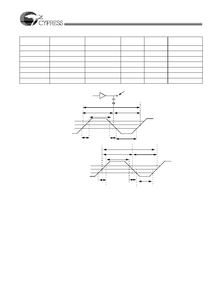
Clock Output Wave
2.5V Clocking
3.3V Clocking
Test Point
Test Load
T
PERIOD
Duty Cycle
T
HIGH
2.0
1.25
0.4
T
LOW
T
RISE
T
FALL
T
LOW
T
RISE
T
FALL
T
PERIOD
Duty Cycle
T
HIGH
2.4
1.5
0.4
Output
Buffer
Interface
Interface
Figure 1. Output Buffer
CY28301
Document #: 38-07011 Rev. *C
Page 14 of 15
© Cypress Semiconductor Corporation, 2002. The information contained herein is subject to change without notice. Cypress Semiconductor Corporation assumes no responsibility for the use
of any circuitry other than circuitry embodied in a Cypress Semiconductor product. Nor does it convey or imply any license under patent or other rights. Cypress Semiconductor does not authorize
its products for use as critical components in life-support systems where a malfunction or failure may reasonably be expected to result in significant injury to the user. The inclusion of Cypress
Semiconductor products in life-support systems application implies that the manufacturer assumes all risk of such use and in doing so indemnifies Cypress Semiconductor against all charges.
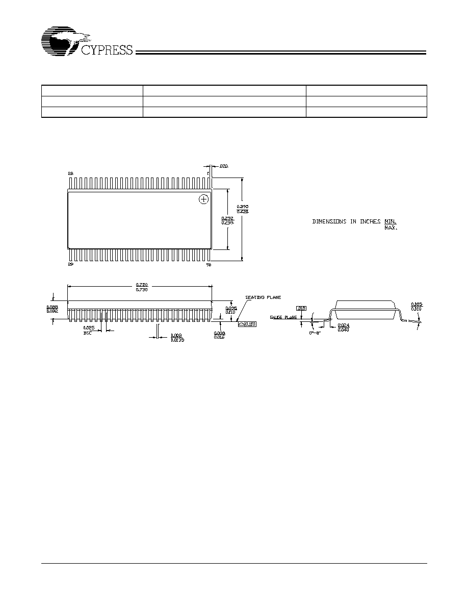
Package Drawing and Dimension
Intel is a registered trademark of Intel Corporation. All product or company names mentioned in this document are the trademarks
of their respective holders.
Ordering Information
Ordering Code
Package Type
Operating Range
CY28301PVC
56-pin SSOP (300 mils)
Commercial, 0∞C to 70∞C
CY28301PVCT
56-pin SSOP (300 mils) - Tape and Reel
Commercial, 0∞C to 70∞C
56-Lead Shrunk Small Outline Package O56
51-85062-*C
CY28301
Document #: 38-07011 Rev. *C
Page 15 of 15
Document History Page
Document Title: CY28301 Frequency Generator for Intel
Æ
Integrated Chipset
Document Number: 38-07011
REV.
ECN
NO.
Issue
Date
Orig. of
Change
Description of Change
**
106533
06/27/01
IKA
Change from Spec #: 38-01096 to 38-07011
Changed I2C to SMBus and Updated Byte Tables
*A
109365
11/06/01
IKA
Revise AC and DC Tables
*B
118785
09/25/02
DMG
Corrected the spread spectrum values in Bits 0 to 2 in Byte 0 (Control
register 0) table to match the device.
Changed the Package Drawing and Dimension to CY Standard.
Added the tape and reel option in the ordering information table.
*C
122717
12/21/02
RBI
Added power up requirements to operating conditions information.