Zero Delay SDR/DDR Clock Buffer
CY28343
Cypress Semiconductor Corporation
∑
3901 North First Street
∑
San Jose
∑
CA 95134
∑
408-943-2600
Document #: 38-07369 Rev. *A
Revised December 26, 2002
Features
∑ Phase-lock loop clock distribution for DDR and SDR
SDRAM applications
∑ One-single-end clock input to 6 pairs DDR outputs or
13 SDR outputs.
∑ External feedback pins FBIN_SDR/FBOUT_SDR are
used to synchronize the outputs to the clock input for
SDR.
∑ External feedback pins FBIN_SDR/FBOUT_SDR are
used to synchronize the outputs to the clock input for
DDR.
∑ SMBus interface enables/disables outputs.
∑ Conforms to JEDEC SDR/DDR specifications
∑ Low jitter, low skew
∑ 48 pin SSOP package
Note:
1.
Pins marked with [*] have internal pull-down resistors. Pins marked with [**] have internal pull-up resistors.
Table 1. Function Table
SELDDR_SDR#
CLKIN
SDRAM(0:12)
DDRT/C(0:5)
FBIN_DDR
FBOUT_DDR
FBIN_SDR
FBOUT_SDR
1= DDR Mode
2.5V
Compatible
OFF
Active
2.5V
Compatible
2.5V
Compatible
Active
2.5V
Compatible
OFF
OFF
0 = SDRAM Mode
3.3V
Compatible
Active
3.3V
Compatible
OFF
OFF
OFF
Active
3.3V
Compatible
Active
3.3V
Compatible
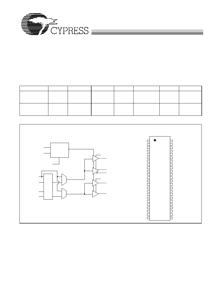
Block Diagram
Pin Configuration
[1]
1
2
3
4
5
6
7
8
9
10
11
12
13
14
15
16
17
18
19
20
21
22
23
24
VDD_3.3V
SDRAM0
SDRAM1
SDRAM2
SDRAM3
VSS
VDD_3.3V
SDRAM4
SDRAM5
CLKIN
SDRAM6
SDRAM7
VSS
VDD_3.3V
SDRAM8
SDRAM9
SDRAM10
SDRAM11
VSS
VDD_3.3V
SDRAM12
FBOUT_SDR
FBIN_SDR*
VSS
48
47
46
45
44
43
42
41
40
39
38
37
36
35
34
33
32
31
30
29
28
27
26
25
SELDDR_SDR#*
FBIN_DDR*
FBOUT_DDR
VDD_2.5V
DDRT5
DDRC5
DDRT4
DDRC4
VSS
VDD_2.5
DDRT3
DDRC3
DDRT2
DDRC2
VSS
VDD_2.5V
DDRT1
DDRC1
DDRT0
DDRC0
VSS
VDD_3.3V
SCLK**
SDATA**
FBOUT_DDR
DDRT(0:5)
DDRC(0:5)
Control
Logic
FBOUT_SDR
SDRAM (0:12)
SCLK
SDATA
PLL
*SELDDR_SDR
FBIN_DDR
CLKIN
FBIN_SDR
VDD_2.5V
VDD_3.3V
VDD_3.3V
CY28343
Document #: 38-07369 Rev. *A
Page 2 of 10
Notes:
2.
PU = internal pull-up PD = internal pull-down.
3.
A bypass capacitor (0.1 mF) should be placed as close as possible to each positive power pin (<0.2"). If these bypass capacitors are not close to the pins their
high frequency filtering characteristic will be cancelled by the lead inductance of the traces.
Power Management
The individual output enable/disable control of the CY28343
allows the user to implement unique power management
schemes into the design. Outputs are in LOW state when dis-
abled through the two-line interface as individual bits are set
LOW in Byte0 to Byte2 registers. The feedback output
FBOUT_DDR and FBOUT_SDR cannot be disabled via
two-line serial bus.
Zero Delay Buffer
When used as a
ZERO
delay buffer the CY28343 will likely be
in a nested clock tree application. For these applications the
CY28343 offers single-end input as a PLL reference. The
CY28343 then can lock onto the reference and translate with
near zero to low-skew outputs. For normal operation, the ex-
ternal feedback input, FBIN_DDR and FBIN_SDR, are con-
nected to the feedback output, FBOUT_DDR and
FBOUT_SDR. By connecting the feedback output to the feed-
back input the propagation delay through the device is elimi-
nated. The PLL works to align the output edge with the input
reference edge thus producing a near zero delay. The refer-
ence frequency affects the static phase offset of the PLL and
thus the relative delay between the inputs and outputs.
Pin Description
[2, 3]
Pin
Name
I/O
Description
10
CLKIN
I
Clock Input. Reference the PLL
47
FBIN_DDR
I
PD
Feedback Clock Output. Connect to FBOUT_DDR for accessing the PLL.
See Function Table on page 1
23
FBIN_SDR
I
PD
Feedback Clock Input. Connect to FBOUT_SDR for accessing the PLL. See
Function Table on page 1
30,32,36,38
42,44
DDRT(0:5)
O
Clock Outputs. True copies of the CLKIN input
29,31,35,37
41,43
DDRC(0:5)
O
Clock Outputs. Complementary copies of the CLKIN input
2-5,8,9
15-18,21
SDRAM(0:12)
O
Clock Outputs. True copies of the CLKIN input
46
FBOUT_DDR
O
Feedback Clock Output. Connect to FBIN_DDR for normal operation. A true
copy of the CLKIN input. The delay of the PCB trace RC at this output will
control Input Reference/DDR Output Clocks phase relationships.
22
FBOUT_SDR
O
Feedback Clock Output. Connect to FBIN_SDR for normal operation. A true
copy of the CLKIN input. The delay of the PCB trace RC at this output will
control Input Reference/ SDR Output Clocks phase relationships.
48
SELDDR_SDR#
I
PD
SDR or DDR Select Pin. See Function Table on page 1
26
SCLK
I
PU
Serial Clock Input. Clocks data at SDATA into the internal register.
25
SDATA
I/O
PU
Serial Data Input. Input data is clocked to the internal register to enable/disable
individual outputs. This provides flexibility in power management.
1,7,14,20,27
VDD_3.3V
3.3V power supply for SDR outputs and two line serial Interface
33,39,45
VDD_2.5V
2.5V power supply for DDR outputs
6,13,19,24,28
,34,40
VSS
Common Ground
CY28343
Document #: 38-07369 Rev. *A
Page 3 of 10
Serial Data Interface
To enhance the flexibility and function of the clock synthesizer,
a two-signal serial interface is provided. Through the Serial
Data Interface, various device functions such as individual
clock output buffers, etc., can be individually enabled or dis-
abled.
The registers associated with the Serial Data Interface initial-
ize to their default setting upon power-up, and therefore use of
this interface is optional. Clock device register changes are
normally made upon system initialization, if any are required.
The interface can also be used during system operation for
power management functions.
Data Protocol
The clock driver serial protocol accepts byte write, byte read,
block write, and block read operation from the controller. For
block write/read operation, the bytes must be accessed in se-
quential order from lowest to highest byte (most significant bit
first) with the ability to stop after any complete byte has been
transferred. For byte write and byte read operations, the sys-
tem controller can access individual indexed bytes. The offset
of the indexed byte is encoded in the command code, as de-
scribed in Table 2.
The block write and block read protocol is outlined in Table 3
while Table 4 outlines the corresponding byte write and byte
read protocol.
The slave receiver address is 11010010 (D2h).
T
Table 2. Command Code Definition
Bit
Description
7
0 = Block read or block write operation
1 = Byte read or byte write operation
(6:0)
Byte offset for byte read or byte write operation. For block read or block write operations, these bits
should be '0000000'
Table 3. Block Read and Block Write Protocol
Block Write Protocol
Block Read Protocol
Bit
Description
Bit
Description
1
Start
1
Start
2:8
Slave address ≠ 7 bits
2:8
Slave address ≠ 7 bits
9
Write
9
Write
10
Acknowledge from slave
10
Acknowledge from slave
11:18
Command Code ≠ 8 Bit'00000000' stands for
block operation
11:18
Command Code ≠ 8 Bit'00000000' stands for
block operation
19
Acknowledge from slave
19
Acknowledge from slave
20:27
Byte Count ≠ 8 bits
20
Repeat start
28
Acknowledge from slave
21:27
Slave address ≠ 7 bits
29:36
Data byte 0 ≠ 8 bits
28
Read
37
Acknowledge from slave
29
Acknowledge from slave
38:45
Data byte 1 ≠ 8 bits
30:37
Byte count from slave ≠ 8 bits
46
Acknowledge from slave
38
Acknowledge
....
Data Byte N/Slave Acknowledge
39:46
Data byte from slave ≠8 bits
....
Data Byte N ≠ 8 bits
47
Acknowledge
....
Acknowledge from slave
48:55
Data byte from slave ≠ 8 bits
....
Stop
56
Acknowledge
....
Data bytes from slave/Acknowledge
....
Data byte N from slave ≠ 8 bits
....
Not Acknowledge
....
Stop
CY28343
Document #: 38-07369 Rev. *A
Page 4 of 10
Note:
4.
These bits will be ignored in DDR mode. See Table 1 on page 1.
Table 4. Byte Read and Byte Write Protocol
Byte Write Protocol
Byte Read Protocol
Bit
Description
Bit
Description
1
Start
1
Start
2:8
Slave address ≠ 7 bits
2:8
Slave address ≠ 7 bits
9
Write
9
Write
10
Acknowledge from slave
10
Acknowledge from slave
11:18
Command Code - 8 bits'1xxxxxxx' stands for
byte operationbit[6:0] of the command code rep-
resents the offset of the byte to be accessed
11:18
Command Code ≠ 8 bits'1xxxxxxx' stands for
byte operationbit[6:0] of the command code rep-
resents the offset of the byte to be accessed
19
Acknowledge from slave
19
Acknowledge from slave
20:27
Byte Count ≠ 8 bits
20
Repeat start
28
Acknowledge from slave
21:27
Slave address ≠ 7 bits
29
stop
28
Read
29
Acknowledge from slave
30:37
Data byte from slave ≠ 8 bits
38
Not Acknowledge
39
stop
Byte 0: Output Register (1 = Enable, 0 = Disable)
[4]
Bit
@Pup
Pin #
Description
7
1
29,30
DDRT/C0. 1 = Enable, 0 = Output disabled asynchronously in a low state
6
1
31,32
DDRT/C1. 1 = Enable, 0 = Output disabled asynchronously in a low state
5
1
35,36
DDRT/C2. 1 = Enable, 0 = Output disabled asynchronously in a low state
4
1
37,38
DDRT/C3. 1 = Enable, 0 = Output disabled asynchronously in a low state
3
1
41,42
DDRT/C4. 1 = Enable, 0 = Output disabled asynchronously in a low state
2
1
43,44
DDRT/C5. 1 = Enable, 0 = Output disabled asynchronously in a low state
1
1
Reserved
0
1
48
SELDDR_DDR hardware setting value. Read only.
Byte 1: Output Register (1 = Enable, 0 = Disable)
[4]
Bit
@Pup
Pin #
Description
7
1
12
SDRAM7. 1 = Enable, 0 = Output disabled asynchronously in a low state
6
1
11
SDRAM6. 1 = Enable, 0 = Output disabled asynchronously in a low state
5
1
9
SDRAM5. 1 = Enable, 0 = Output disabled asynchronously in a low state
4
1
8
SDRAM4. 1 = Enable, 0 = Output disabled asynchronously in a low state
3
1
5
SDRAM3. 1 = Enable, 0 = Output disabled asynchronously in a low state
2
1
4
SDRAM2. 1 = Enable, 0 = Output disabled asynchronously in a low state
1
1
3
SDRAM1. 1 = Enable, 0 = Output disabled asynchronously in a low state
0
1
2
SDRAM0. 1 = Enable, 0 = Output disabled asynchronously in a low state
CY28343
Document #: 38-07369 Rev. *A
Page 5 of 10
Byte 2: Output Register (1 = Enable, 0 = Disable)
[4]
Bit
@Pup
Pin #
Description
7
1
Reserved for device test.
6
1
Select drive strength for SDR outputs. 1 = Low drive, 0 = High drive
5
1
Reserved
4
1
21
SDRAM12. 1 = Enable, 0 = Output disabled asynchronously in a low state
3
1
18
SDRAM11. 1 = Enable, 0 = Output disabled asynchronously in a low state
2
1
17
SDRAM10. 1 = Enable, 0 = Output disabled asynchronously in a low state
1
1
16
SDRAM9. 1 = Enable, 0 = Output disabled asynchronously in a low state
0
1
15
SDRAM8. 1 = Enable, 0 = Output disabled asynchronously in a low state
Byte 3: Silicon Register (Read Only)
Bit
@Pup
Pin #
Description
7
1
Vendor ID
1000 Cypress
6
0
5
0
4
0
3
0
Revision ID
2
0
1
0
0
0