 | –≠–ª–µ–∫—Ç—Ä–æ–Ω–Ω—ã–π –∫–æ–º–ø–æ–Ω–µ–Ω—Ç: CY28354OC | –°–∫–∞—á–∞—Ç—å:  PDF PDF  ZIP ZIP |

200-MHz 24-Output Buffer for 4 DDR DIMMS
CY28354
Cypress Semiconductor Corporation
∑
3901 North First Street
∑
San Jose
∑
CA 95134
∑
408-943-2600
Document #: 38-07423 Rev. *A
Revised December 19, 2002
Features
∑ Dual 1- to 12-output buffer/driver
∑ Supports up to 4 DDR DIMMs
∑ Outputs are individually enabled/disabled
∑ Low-skew outputs (< 100 ps)
∑ Supports 266-MHz, 333-MHz and 400-MHz DDR SDRAM
∑ SMBus Read and Write support
∑ Space-saving 48-pin SSOP package
Functional Description
The CY28354 is a 2.5V buffer designed to distribute
high-speed clocks in PC applications. The part has 24 outputs.
Designers can configure these outputs to support four unbuf-
fered DDR DIMMS or to support 3 unbuffered standard
SDRAM DIMMs and 2 DDR DIMMS. The CY28354 can be
used in conjunction with the W250 or similar clock synthesizer
for the VIA Pro 266 chipset.
The CY28354 also includes an SMBus interface which can
enable or disable each output clock. On power-up, all output
clocks are enabled.
Block Diagram
BUF_INA
SDATA
SCLOCK
1
2
3
4
VDD2.5
GND
NC
NC
DDRBT2
DDRBC2
DDRBT3
DDRBC3
SSOP
Top View
Pin Configuration
8
5
6
7
12
9
10
11
13
14
15
16
20
17
18
19
24
21
22
23
48
47
46
45
41
44
43
42
37
40
39
38
36
35
34
33
29
32
31
30
25
28
27
26
DDRAT4
DDRAC4
DDRAT5
DDRAC5
DDRBT4
DDRBC4
DDRBT5
DDRBC5
VDD2.5
SDATA
SCLK
VDD2.5
GND
FB_OUTB
BUFF_INB
DDRBT0
DDRBC0
DDRBT1
DDRBC1
VDD2.5
DDRAT0
DDRAC0
DDRAT1
DDRAC1
GND
VDD2.5
FB_OUTA
BUF_INA
DDRAT2
DDRAC2
DDRAT3
DDRAC3
VDD2.5
GND
GND
BUFF_INB
DDRBT0
DDRBC0
DDRBT1
DDRBC1
DDRAT0
DDRAC0
DDRAT1
DDRAC1
DDRAT2
DDRAC2
DDRAT3
DDRAC3
FB_OUTA
FB_OUTB
DDRBT2
DDRBC2
DDRBT3
DDRBC3
DDRBT4
DDRBC4
DDRBT5
GND
VDD2.5
VDD2.5
GND
DDRBC5
DDRAT4
DDRAC4
DDRAT5
DDRAC5
GND
SMBus
Decoding
CY28354
Document #: 38-07423 Rev. *A
Page 2 of 10
Pin Description
Pin
Name
PWR
I/O
Description
11, 13, 19, 21, 38, 36,
5, 7, 44, 42, 32, 30
DDRA[0:5]T
DDRB[0:5]T
VDD2.5
O
Clock outputs. These outputs provide copies of
BUF_INA & BUF_INB, respectively.
12, 14, 20, 22, 37, 35,
6, 8, 43, 41, 31, 29
DDRA[0:5]C
DDRB[0:5]C
VDD2.5
O
Clock outputs. These outputs provide complemen-
tary copies of BUF_INA & BUF_INB, respectively.
18,
4
BUF_INA,
BUF_INB
VDD2.5
I
Reference input from chipset. 2.5V input.
17,
3
FB_OUTA
FB_OUTB
VDD2.5
O
Feedback clock for chipset
46, 45
NC
Not Connected
25
SCLK
VDD2.5
I
SMBus clock input
26
SDATA
VDD2.5
I/O
SMBus data input
1, 10, 16, 23, 28, 33, 39, 48
VDD2.5
2.5V voltage supply
2, 9, 15, 24, 27, 34, 40, 47
GND
Ground
CY28354
Document #: 38-07423 Rev. *A
Page 3 of 10
Serial Data Interface
To enhance the flexibility and function of the clock synthesizer,
a two-signal serial interface is provided. Through the Serial
Data Interface, various device functions such as individual
clock output buffers, etc., can be individually enabled or dis-
abled. The registers associated with the Serial Data Interface
initializes to their default setting upon power-up, and therefore
use of this interface is optional. Clock device register changes
are normally made upon system initialization, if any are re-
quired. The interface can also be used during system opera-
tion for power management functions.
Data Protocol
The clock driver serial protocol accepts byte write, byte read,
block write, and block read operation from the controller. For
block write/read operation, the bytes must be accessed in se-
quential order from lowest to highest byte (most significant bit
first) with the ability to stop after any complete byte has been
transferred. For byte write and byte read operations, the sys-
tem controller can access individual indexed bytes. The offset
of the indexed byte is encoded in the command code, as de-
scribed in Table 1. The block write and block read protocol is
outlined in Table 2.The slave receiver address is D2 depend-
ing on the state of the ADDRSEL pin.
T
Table 1. Command Code Definition
Bit
Description
7
0 = Block read or block write operation
1 = Byte read or byte write operation
(6:0)
Byte offset for byte read or byte write operation. For block read or block write operations, these bits should
be '0000000'
Table 2. Block Read and Block Write protocol
Block Write Protocol
Block Read Protocol
Bit
Description
Bit
Description
1
Start
1
Start
2:8
Slave address ≠ 7 bits
2:8
Slave address ≠ 7 bits
9
Write = 0
9
Write = 0
10
Acknowledge from slave
10
Acknowledge from slave
11:18
Command Code ≠ 8 bits
'00000000' stands for block operation
11:18
Command Code ≠ 8 bits
'00000000' stands for block operation
19
Acknowledge from slave
19
Acknowledge from slave
20:27
Byte Count from master ≠ 8 bits
20
Repeat start
28
Acknowledge from slave
21:27
Slave address ≠ 7 bits
29:36
Data byte 0 from master ≠ 8 bits
28
Read = 1
37
Acknowledge from slave
29
Acknowledge from slave
38:45
Data byte 1 from master ≠ 8 bits
30:37
Byte count from slave ≠ 8 bits
46
Acknowledge from slave
38
Acknowledge
....
Data bytes from master/Acknowledge
39:46
Data byte 0 from slave ≠ 8 bits
....
Data Byte N ≠ 8 bits
47
Acknowledge
....
Acknowledge from slave
48:55
Data byte 1 from slave ≠ 8 bits
....
Stop
56
Acknowledge
....
Data bytes from slave/Acknowledge
....
Data byte N from slave ≠ 8 bits
....
Not Acknowledge
....
Stop
CY28354
Document #: 38-07423 Rev. *A
Page 4 of 10
Serial Configuration Map
∑ The Serial bits will be read by the clock driver in the following
order:
Byte 0 - Bits 7, 6, 5, 4, 3, 2, 1, 0
Byte 1 - Bits 7, 6, 5, 4, 3, 2, 1, 0
Byte N - Bits 7, 6, 5, 4, 3, 2, 1, 0
∑ Reserved and unused bits should be programmed to "0".
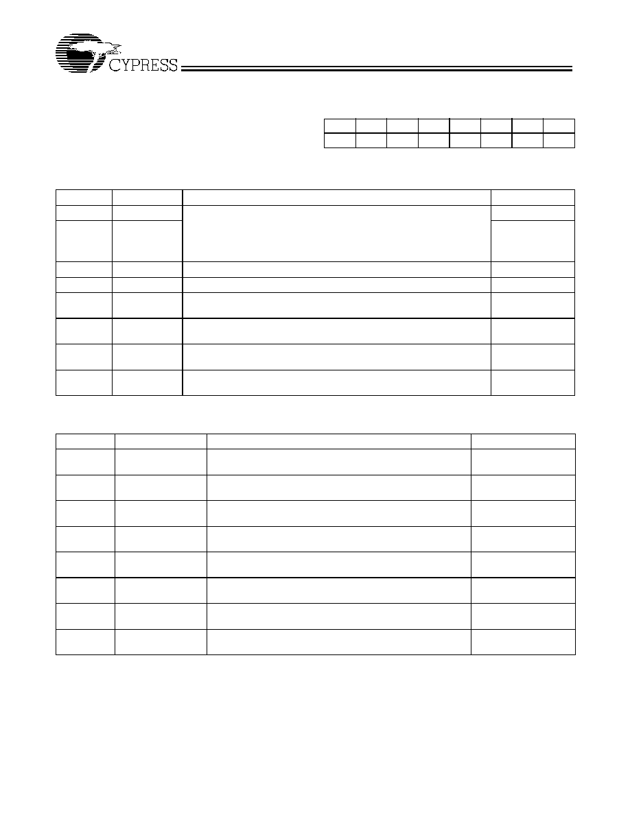
∑ SMBus Address for the CY28354 is:
∑
A6
A5
A4
A3
A2
A1
A0
R/W
1
1
0
1
0
0
1
----
Byte 0: Outputs Active/Inactive Register (1 = Active, 0 = Inactive), Default = Active
Bit
Pin #
Description
Default
Bit 7
Input Threshold Control
00: Normal (1.25V)
01: 1.20V
10: 1.15V
11: 1.35V
0
Bit 6
0
Bit 5
17
FBOUTA Control, 0 = Enable, 1 = Disable
0
Bit 4
3
FBOUTB Control, 0 = Enable, 1 = Disable
0
Bit 3
30,
29
DDRBT5,
DDRBC5
1
Bit 2
32,
31
DDRBT4,
DDRBC4
1
Bit 1
42,
41
DDRBT3,
DDRBC3
1
Bit 0
44,
43
DDRBT2,
DDRBC2
1
Byte 1: Outputs Active/Inactive Register (1 = Active, 0 = Inactive), Default = Active
Bit
Pin #
Description
Default
Bit 7
7,
8
DDRBT1,
DDRBC1
1
Bit 6
5,
6
DDRBT0,
DDRBC0
1
Bit 5
36,
35
DDRAT5,
DDRAC5
1
Bit 4
38,
37
DDRAT4,
DDRAC4
1
Bit 3
21,
22
DDRAT3,
DDRAC3
1
Bit 2
19,
20
DDRAT2,
DDRAC2
1
Bit 1
13,
14
DDRAT1,
DDRAC1
1
Bit 0
11,
12
DDRAT0,
DDRAC0
1
CY28354
Document #: 38-07423 Rev. *A
Page 5 of 10
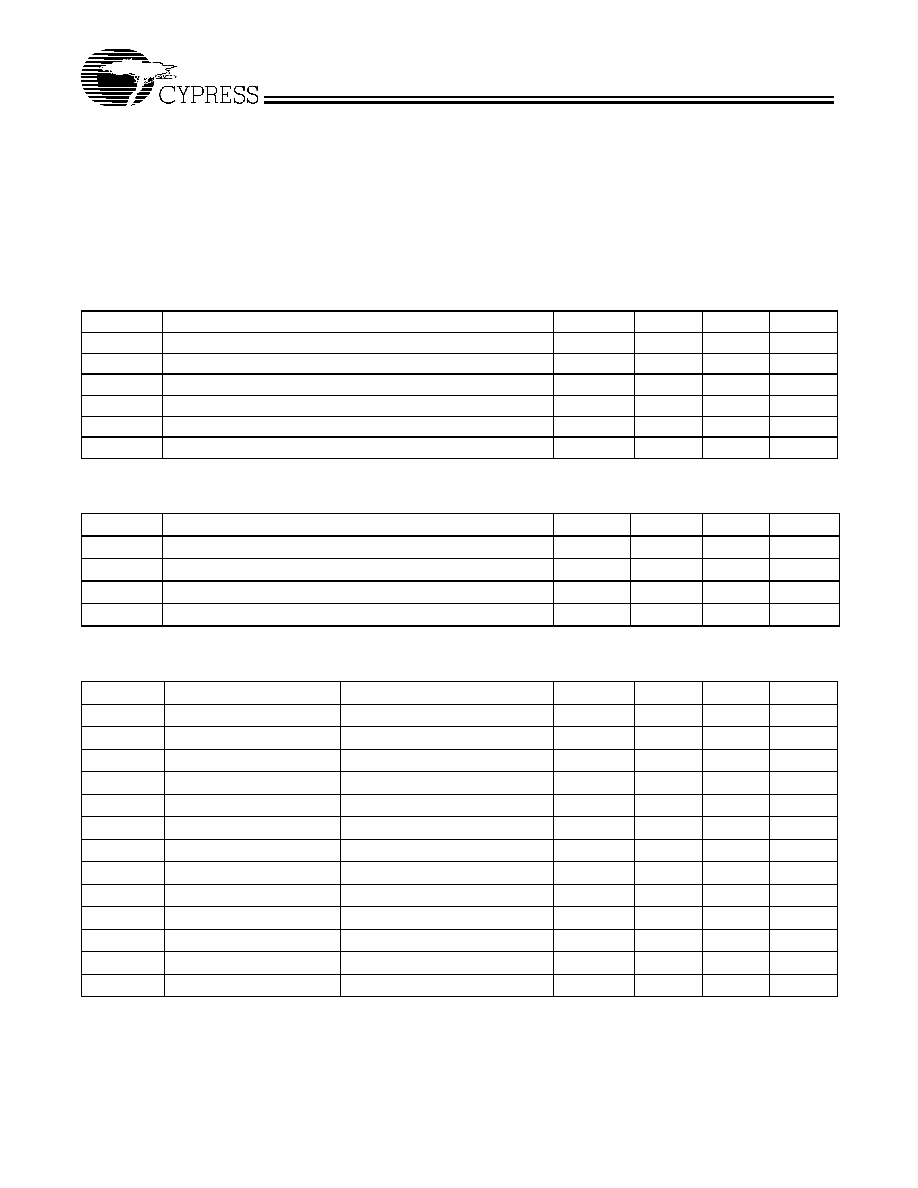
Absolute Maximum Ratings
[1]
Supply Voltage to Ground Potential ..................≠0.5 to +7.0V
DC Input Voltage (except BUF_IN) ............ ≠0.5V to V
DD
+0.5
Storage Temperature .................................. ≠65∞C to +150∞C
Static Discharge Voltage ............................................>2000V
(per MIL-STD-883, Method 3015)
This device contains circuitry designed to protect the inputs
against damage due to high static voltages or electric field;
however, precautions should be taken to avoid application of
any voltage higher than the maximum rated voltages to this
circuit. For proper operation, V
in
and V
out
should be con-
strained to the range:
V
SS
< (V
in
or V
out
) < V
DD
Unused inputs must always be tied to an appropriate logic volt-
age level (either V
SS
or V
DD
).
Table 3. Absolute Maximum Ratings
Parameter
Description
Min.
Typ.
Max.
Unit
V
DD
Supply Voltage to Ground Potential
≠0.5
7.0
V
V
in
DC Input Voltage (except BUFF_IN)
≠0.5
V
DD
+0.5
V
V
out
Output Voltage
T
s
Temperature, Storage
≠65
+150
∞C
T
a
Temperature, Operating Ambient
0
70
∞C
ESD
h
ESD Protection (Human Body Model)
2000
V
Table 4. DC Parameter
Parameter
Description
Min.
Typ.
Max.
Unit
V
DD2.5
Supply Voltage
2.375
2.625
V
T
A
Operating Temperature (Ambient Temperature)
0
70
∞C
C
OUT
Output Capacitance
6
pF
C
IN
Input Capacitance
5
pF
Table 5. Electrical Characteristics Over the Operating Range
Parameter
Description
Conditions
Min.
Typ.
Max.
Unit
V
IL
Input LOW Voltage
For all pins except SMBus
0.8
V
V
IH
Input HIGH Voltage
2.0
V
I
IL
Input LOW Current
V
IN
= 0V
50
µ
A
I
IH
Input HIGH Current
V
IN
= V
DD
50
µ
A
I
OH
Output HIGH Current
V
DD
= 2.375V, V
OUT
= 1V
≠18
≠32
mA
I
OL
Output LOW Current
V
DD
= 2.375V, V
OUT
= 1.2V
26
35
mA
V
OL
Output LOW Voltage
[2]
I
OL
= 12 mA, V
DD
= 2.375V
0.6
V
V
OH
Output HIGH Voltage
[2]
I
OH
= ≠12 mA, V
DD
= 2.375V
1.7
V
I
DD
Supply Current
[2]
Unloaded outputs, 133 MHz
400
mA
I
DD
Supply Current
Loaded outputs, 133 MHz
500
mA
V
OUT
Output Voltage Swing
See Test Circuity. See Figure 1
0.7
V
DD
+ 0.6
V
V
OC
Output Crossing Voltage
1.0
1.25
1.5
V
IN
DC
Input Clock Duty Cycle
48
52
%
Note:
1.
Multiple Supplies: The Voltage on any input or I/O pin cannot exceed the power pin during power-up. Power supply sequencing is NOT required.
2.
Parameter is guaranteed by design and characterization. Not 100% tested in production.