/home/web/doc/html/cypress/169303
200-MHz, Ten-output Zero Delay Buffer/PLL
CY292510
Cypress Semiconductor Corporation
·
3901 North First Street
·
San Jose
·
CA 95134
·
408-943-2600
Document #: 38-07472 Rev. **
Revised October 11, 2002
Features
· Output frequency range: 25 MHz to 200 MHz
· 10 LVCMOS outputs
· One feedback output
· Output-to-output skew < 100 ps
· Cycle-to cycle jitter < 100 ps
· ± 125-ps static phase error: 66 MHz to 166 MHz
· Spread-Spectrum-compatible
· Integrated series damping resistors specifically
designed for registered SDRAM DIMM applications
JEDEC-JC42.5-compliant
· Externally controllable output delay
· Output enable/disable control
· 24-pin TSSOP package
Description
The CY292510 is a 3.3V zero delay buffer designed to
distribute high-speed clocks in PC, workstation, datacom,
telecom, and other high-performance applications. It is ideal
for use in SDRAM memory applications, and conforms to the
JEDEC JC40/JC42.5 specification supporting SDRAM DIMM
applications.
The CY292510 has one bank of outputs with output enable
control. Input-to-output skew can be adjusted by varying
load/delay on feedback path. When OE is low, clock outputs
are forced low. V
DDA
can be strapped low to force device into
test mode. See Table 4.
Note:
1.
See Table 4 for additional logic configurations. REF is fixed frequency input.
Table 1. Function Table
[1]
OE
1Y(0:9) Outputs
FBOUT
LOW
LOW
REF
HIGH
REF
REF
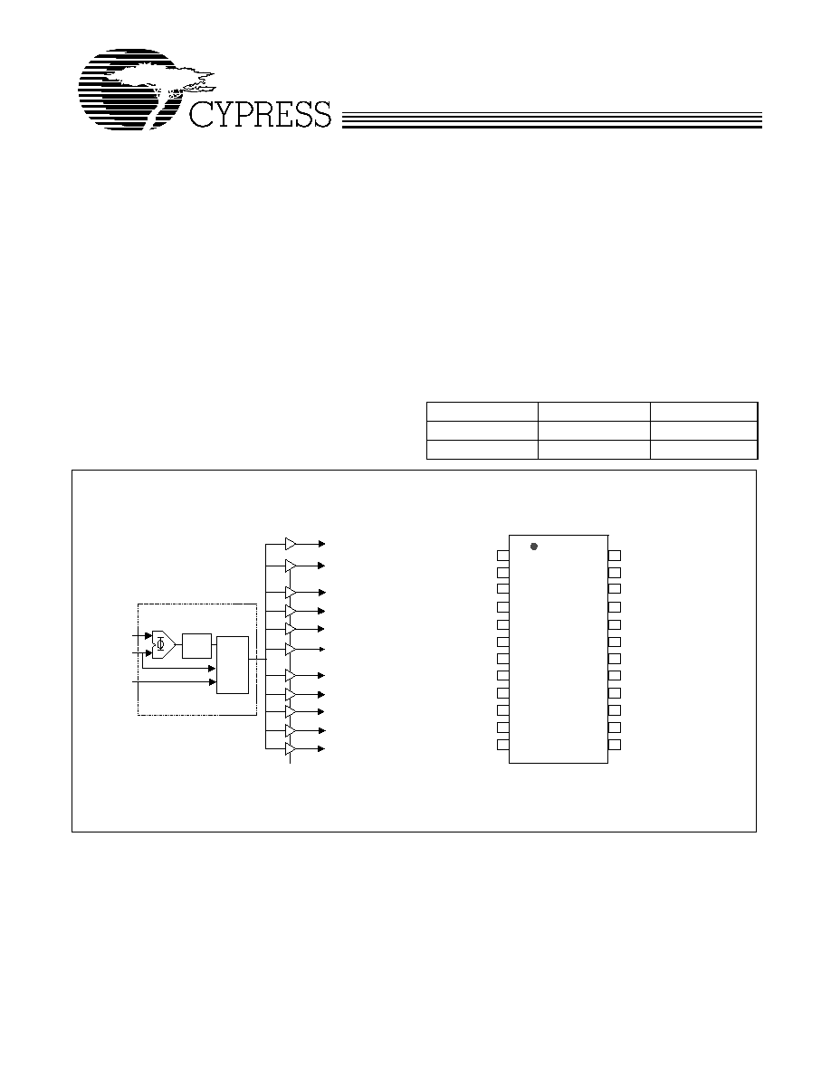
Block Diagram
Pin Configuration
1
MUX
0
SEL
FBIN
REF
VDDA
1Y9
1Y8
1Y7
1Y6
1Y5
OE
1Y3
1Y2
1Y1
1Y0
FBOUT
1Y4
PLL
V
SSA
V
DD
1Y0
1Y1
1Y2
V
SS
V
SS
1Y3
1Y4
V
DD
OE
FBOUT
1
2
3
4
5
6
7
8
9
10
11
12
24
23
22
21
20
19
18
17
16
15
14
13
REF
V
DDA
V
DD
1Y9
1Y8
V
SS
V
SS
1Y7
1Y6
1Y5
V
DD
FBIN
CY292510
Document #: 38-07472 Rev. **
Page 2 of 6
Notes:
2.
Stresses beyond those listed under " absolute maximum ratings" may cause permanent damage to the device. These are stresses rating only and functional
operation of the device at these or any other conditions beyond those indicated under " recommended operating conditions" is not implied. Exposure to
absolute-maximum-rated conditions for extended periods may affect device reliability.
3.
The input and output negative-voltage ratings may be exceeded if the input and output clamp-current ratings are observed.
4.
The maximum package power dissipation is calculated using a junction temperature or 150°C and board trace length of 750 mils.
5.
Unused inputs must be held high or low to prevent them from floating.
Pin Description
Pin
Name
I/O
Description
24
REF
I
Input reference pin.
12
FBOUT
O
Feedback Output. Not affected by the OE pin.
13
FBIN
I
This pin is to be connected to the FBOUT pin. A timing delay may be inserted to change the
delay through the device.
11
OE
I
Output Enable clock (high active). OE low places CLK(0:9) into low state. See Block Diagram.
2, 10, 14, 22
V
DD
PWR 3.3V supply for core logic, inputs and outputs.
23
V
DDA
PWR Power for internal analog circuitry. This supply should have separate de coupling. For test
purposes, when V
DDA
is strapped to ground the internal PLL is shut off and bypassed and
REF is buffered directly to device outputs( see Table 4).
3, 4, 5, 8, 9, 15,
16, 17, 20, 21
1Y(0:9)
O
Low skew clock outputs. Outputs enabled by OE in high state.
6, 7, 18, 19
V
SS
PWR Ground pins for the core logic and I/Os.
1
V
SSA
PWR Ground pin for analog circuitry.
Table 2. Absolute Maximum Ratings
[2]
Parameter
Description
Commercial
Unit
V
DD
, V
DDA
Supply Voltage Range
0.5 to +4.6
V
V
I
[3]
Input Voltage Range
0.5 to V
DD
+ 0.5
V
V
O
[3]
Voltage range applied to any output in the high or low state 0.5 to V
DD
+0.5
V
I
IK
(VI<0)
Input clamp current
50
mA
I
OK
(V
O
<0 or V
O
>V
DD
Terminal voltage with respect to V
SS
(inputs V
IH
2.5, V
IL
2.5 ±50
mA
I
O
(V
O
= 0 to V
DD
)
Continuous Output Current
±50
mA
V
DD
or V
SS
Continuous Current
±100
mA
T
A
= 50°C (in still air)
[4]
Maximum power dissipation
0.7
W
T
STG
Storage Temperature Range
65°C to +150°C
°C
Table 3. Capacitance
[5]
Parameter
Description
Min.
Typ.
Max.
Unit
C
IN
Input Capacitance V
IN
= V
DD
or V
SS
5
pF
C
O
Output Capacitance V
O
= V
DD
or V
SS
6
pF
Table 4. Test Mode Table (V
DDA
= 0V)
INPUTS
OUTPUTS
OE
REF
1Y(0:9)
FBOUT
LOW
LOW
LOW
LOW
LOW
HIGH
LOW
HIGH
HIGH
LOW
LOW
LOW
HIGH
HIGH
HIGH
HIGH
CY292510
Document #: 38-07472 Rev. **
Page 3 of 6
Table 5. Recommended Operating Conditions
Parameter
Description
Min.
Typ.
Max.
Unit
V
DD
Supply voltage
3.0
3.3
3.6
V
V
DDA
Analog supply voltage
3.0
3.3
3.6
V
V
IN
Voltage applied to input pins
0
V
DD
V
I
OH
High level output current
12
mA
I
OL
Low level output current
12
mA
T
A
Operating free-air temperature
0
85
°C
Table 6. DC Parameters (V
DD
= V
DDA
= 3.3V ±10%, T
A
= 0°C to +85°C)
Parameter
Description
Test Conditions
Min.
Typ.
Max.
Unit
V
IH
HIGH Level input voltage
2.0
V
V
IL
LOW level input voltage
0.8
V
V
OH
HIGH level output voltage
Min. to Max.
I
OH
=
100
µ
A
V
DD
0.2
V
V
DD
= 3V
I
OH
= 12 mA
2.1
V
DD
= 3V
I
OH
= -6 mA
2.4
V
OL
LOW level output voltage
Min. to Max.
I
OL
=100
µ
A
0.2
V
V
DD
= 3V
I
OL
= 12 mA
0.8
V
DD
= 3V
I
OL
= 6 mA
0.55
I
OH
HIGH level output current
V
DD
= 3.135V
V
O
= 1V
32
mA
V
DD
= 3.3V
V
O
= 1.65V
36
V
DD
= 3.465V
V
O
= 3.135V
12
I
OL
LOW level output current
V
DD
= 3.135V
V
O
= 1.95V
34
mA
V
DD
= 3.3V
V
O
= 1.65V
40
V
DD
= 3.465V
V
O
= 0.4V
14
V
IK
Clamp voltage
V
DD
= 3V
I
IN
= 18 mA
1.2
V
I
I
Input leakage current per pin V
DD
= 3.6V
V
I
= V
DD
or V
SS
±5
µ
A
I
DDA
PLL supply current
Min. to Max.
2.3
3.5
mA
I
DDQ
Quiescent supply current
V
DD
= 3.6V
I
O
= 0 V
IN
= V
DD
or V
SS
5
mA
I
DDQ
Change in quiescent current V
DD
= 3.3 V to 3.6V One input at V
DD
0.6V,
other inputs at V
DD
or
V
SS
500
µ
A
I
DD
Dynamic supply current
V
DD
= 3.6V
Outputs loaded at 133 MHz
200
mA
Table 7. AC Parameters (V
DD
= V
DDA
= 3.3V ±10%, T
A
= 0°C to +85°C)
[6, 7, 8, 9, 10]
Parameter
From Input/Condition
To Output
V
DD
= 3.3V ± 0.3V
Unit
Min.
Typ.
Max.
Fin
Reference Clock
25
200
MHz
Duty Cycle
Reference Clock
40
60
%
Fout
Output Operating Frequency
30-pF load
25
185
MHz
25-pF load
25
200
tPHASE error
[11]
, static
offset (normalized)
REF = 66 to 166 MHz
FBIN
125
125
pS
Duty Cycle
Any clock out or FBOUT
45
55
%
Notes:
6.
Parameters are guaranteed by design and characterization and are not 100% production tested.
7.
The tSK(0) specification is only valid for equal loading of all outputs (30 pF//500
) for Fout < 185 MHz and (25 pF//500
) for Fout > 185 MHz.
8.
The test load is 30 pF//500
for Fout < 185 MHz and 25 pF//500
for Fout > 185 MHz.
9.
See Figure 2.
10. OE = V
DD
.
11.
Uses the averaging feature of the scope to remove the jitter component.
CY292510
Document #: 38-07472 Rev. **
Page 4 of 6
Parameter Measurement Information
Notes:
12. Time required for the integrated PLL circuit to obtain phase lock of its feedback signal to its reference signal. For phase lock to be obtained, a fixed-frequency
fixed-phase reference signal must be present at CLK. Until phase lock is obtained, the specifications for propagation delay, skew and jitter parameters given in
the switching characteristics table are not applicable.
13. t
R
/t
F
are measured at 0.4V to 2.0V.
14. C
L
includes probe and jig capacitance.
15. All input pulses are supplied by generators having the following characteristics: input frequency
100 MHz, Zo = 50
, tr
1.2 ns, tf
<
1.2 ns.
16. The outputs are measured one at a time with one transition per measurement.
tsk(o)
[6,7,9]
Skew, Output to Output
Any clock out
100
pS
Jitter(cycle-to-cycle)
Any clock out or FBOUT
75
pS
t
R
[13]
Any clock out or FBOUT
0.5
2.2
nS
t
F
[13]
Any clock out or FBOUT
0.5
2.2
nS
t
PD
(propagation delay
- bypass mode)
REF
Any clock out or FBOUT
3
ns
T
STABIL
[12]
Stabilization time
FBOUT
1
mS
Table 7. AC Parameters (V
DD
= V
DDA
= 3.3V ±10%, T
A
= 0°C to +85°C) (continued)
[6, 7, 8, 9, 10]
From Output
Under Test
30 pF
500 Ohm
Output
VOH
VOL
2 V
0.4 V
50% VDD
2 V
0.4 V
tr
tf
Load Circuit for Outputs
25 pF load w hen Fout > 185 MHz
Output Rise/Fall Time
Figure 1. Load Circuit and Voltage Waveforms
[14, 15, 16]
CLKIN
FBIN
FBOUT
Any Y
Any Y
Any Y
t
phase error
t
sk(o)
t
sk(o)
Figure 2. Phase Error and Skew Calculations
CY292510
Document #: 38-07472 Rev. **
Page 5 of 6
© Cypress Semiconductor Corporation, 2002. The information contained herein is subject to change without notice. Cypress Semiconductor Corporation assumes no responsibility for the use
of any circuitry other than circuitry embodied in a Cypress Semiconductor product. Nor does it convey or imply any license under patent or other rights. Cypress Semiconductor does not authorize
its products for use as critical components in life-support systems where a malfunction or failure may reasonably be expected to result in significant injury to the user. The inclusion of Cypress
Semiconductor products in life-support systems application implies that the manufacturer assumes all risk of such use and in doing so indemnifies Cypress Semiconductor against all charges.
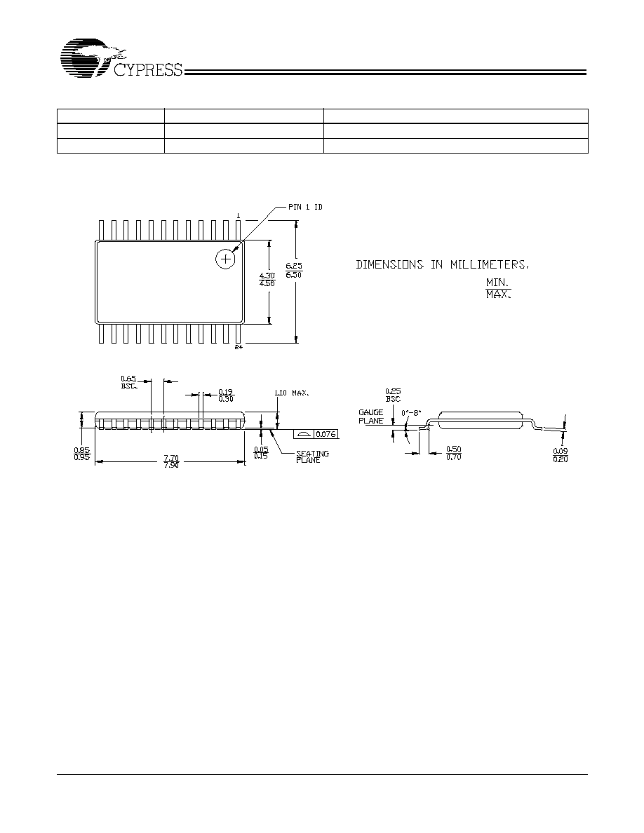
Package Drawing and Dimension
All product and company names mentioned in this document are the trademarks of their respective holders.
Ordering Information
Part Number
Package Type
Production Flow
CY292510ZC
24-pin TSSOP
Commercial, 0°C to +85°C
CY292510ZCT
24-pin TSSOPTape and Reel
Commercial, 0°C to +85°C
24-lead Thin Shrunk Small Outline Package (4.40-mm Body) Z24
51-85119-**