/home/web/doc/html/cypress/169323
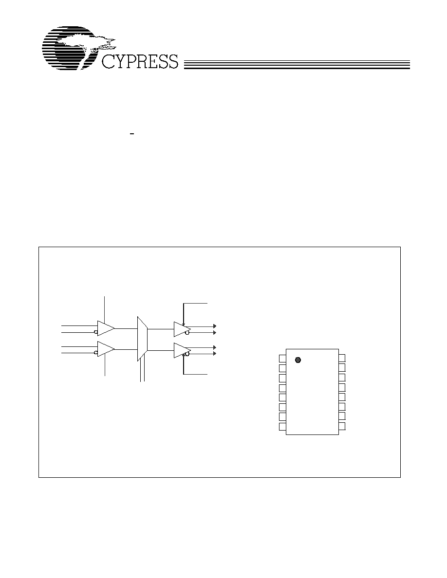
High-drive Two-Channel LVDS Repeater/Mux
ComLinkTM Series
CY2LL843
Cypress Semiconductor Corporation
·
3901 North First Street
·
San Jose
·
CA 95134
·
408-943-2600
Document #: 38-07066 Rev. *A
Revised December 14, 2002
Features
· ANSI TIA/EIA-644-1995-compliant
· Designed for data rates to > 700 Mbs = (350 MHz)
· Single 2 × 2 with high-drive output drivers
· Low -voltage differential signaling with output voltages
of ± 350 mV into 50-ohm load version (Bus LVDS)
· Single 3.3V supply
· Accepts ± 350-mV differential inputs
· Output Drivers are high-impedance when disabled or
when V
DD
1.5V
· 16-pin SOIC/TSSOP packages
· Industrial version available
Description
The Cypress CY2LL843 are differential line drivers and
receivers that utilize Low Voltage Signaling or LVDS, to
achieve signaling rates of 700Mbs. The receiver outputs can
be switched to either or both drivers through the multiplexer
control signals S0/S1. This provides flexibility in application for
either a splitter or router configuration with a single device.
The Cypress CY2LL843 are configured as a single
two-channel repeater/Mux.
The LVDS standard provides a minimum differential output
voltage of 247 mV into a 50-ohm load and receipt of as little as
100 mV signals with up to 1V of DC offset between transmitter
and receiver. The Cypress CY2LL843 doubles the output drive
current to achieve BusLVDS signaling levels with a faster
rise/fall times into 50-ohm load.
A doubly terminated BusLVDS line enables multipoint config-
urations.
Designed for both point to point based-band multi-point data
transmission over controlled impedance lines.
Block Diagram
Pin Configuration
1Y
1Z
2Y
2Z
VDD
1A
1B
2A
2B
GND
1DE
2DE
S0
S1
16 pin SOIC/TSSOP
1
2
3
4
5
6
7
8
16
15
14
13
12
11
10
9
VDD
VDD
1Y
1Z
2DE
2Z
2Y
GND
1B
1A
S0
1DE
S1
2A
2B
GND
CY2L
L
843
ComLinkTM Series
CY2LL843
Document #: 38-07066 Rev. *A
Page 2 of 13
Notes:
1.
See Figure 1.
2.
Stresses greater than those listed under absolute maximum ratings may cause permanent damage to the device. This is intended to be a stress rating only and
functional operation of the device at these or any other conditions above those indicated in the operation sections of this specification is not implied. Exposure
to absolute maximum rating conditions for extended periods may affect reliability.
3.
Multiple Supplies: The voltage on any input or I/O pin cannot exceed the power pin during power-up. Power supply sequencing is NOT required
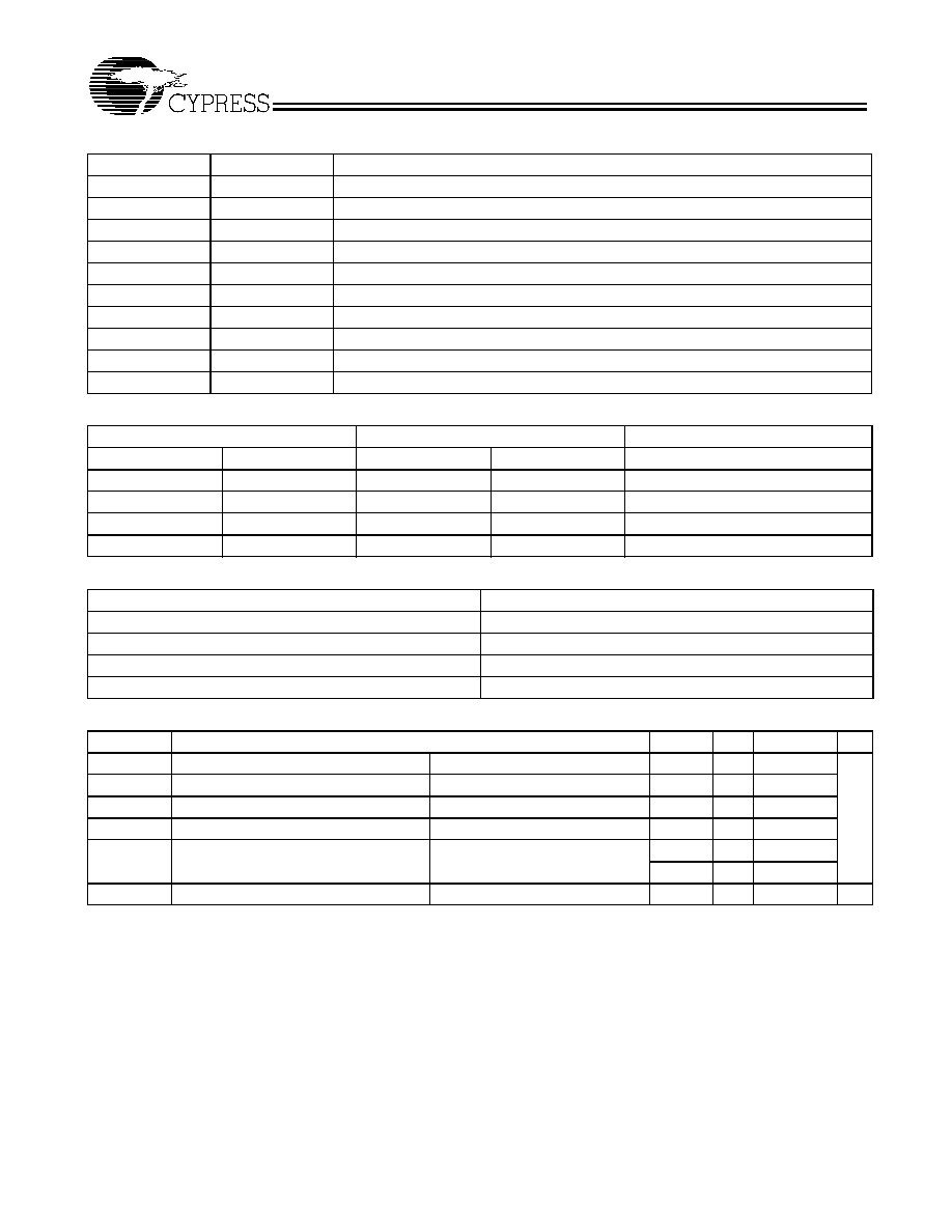
Pin Description
Pin Number
Pin Name
Pin Description
1,2
1B, 1A
Differential Input Channel 1
3
S0
Function Select 0
4
1DE
Data Enable Channel 1
5
S1
Function Select 1
6,7
2A, 2B
Differential Input Channel 2
8,9
G
ND
Ground
10,11
2Y, 2Z
Differential Output Channel 2
12
2DE
Data Enable Channel 2
14,13
IY, 1Z
Differential Output Channel 1
15,16
V
DD
Supply Voltage
Table 1. Mux Function Table
Input
Output
[[1]]
Function
S0
S1
1Y/1Z
2Y/2Z
0
0
1A/1B
1A/1B
Splitter A
1
0
2A/2B
2A/2B
Splitter B
0
1
1A/1B
2A/2B
Pass-thru Router
1
1
2A/2B
1A/1B
Cross Point Router
Table 2. Absolute Maximum Rating Over Operating Free-Air Temperature
[[2]]
Supply Voltage Range, V
DD
(1)
0.5V to 4V
Voltage Range (DE,S0,S1)
0.5V to 6.0V
Input Voltage Range, V
IN
(A or B)
0.5V to V
DD
+ 0.5V
ESD (All pins)
Class 3, A: 2KV, B: 500V
Storage Temperature Range
65°C to 150°C
Table 3. Recommended Operating Conditions
[3]
Parameter
Description
Min. Typ.
Max.
Unit
V
DD
Supply Voltage
3
3.3
3.6
V
V
IH
High Level Input Voltage
(S0,S1,1DE,2DE)
2
V
IL
Low Level Input Voltage
(S0,S1,1DE,2DE)
0.8
V
ID
Magnitude of Differential Input Voltage
0.1
0.6
V
IC
Common Mode Input Voltage
( see Figure 11,Figure 12,
Figure 13)
V
ID
/2
2.4 (V
ID
/2)
VDD 0.8
T
A
Operating Free Air Temperature
40
85
°C
ComLinkTM Series
CY2LL843
Document #: 38-07066 Rev. *A
Page 3 of 13
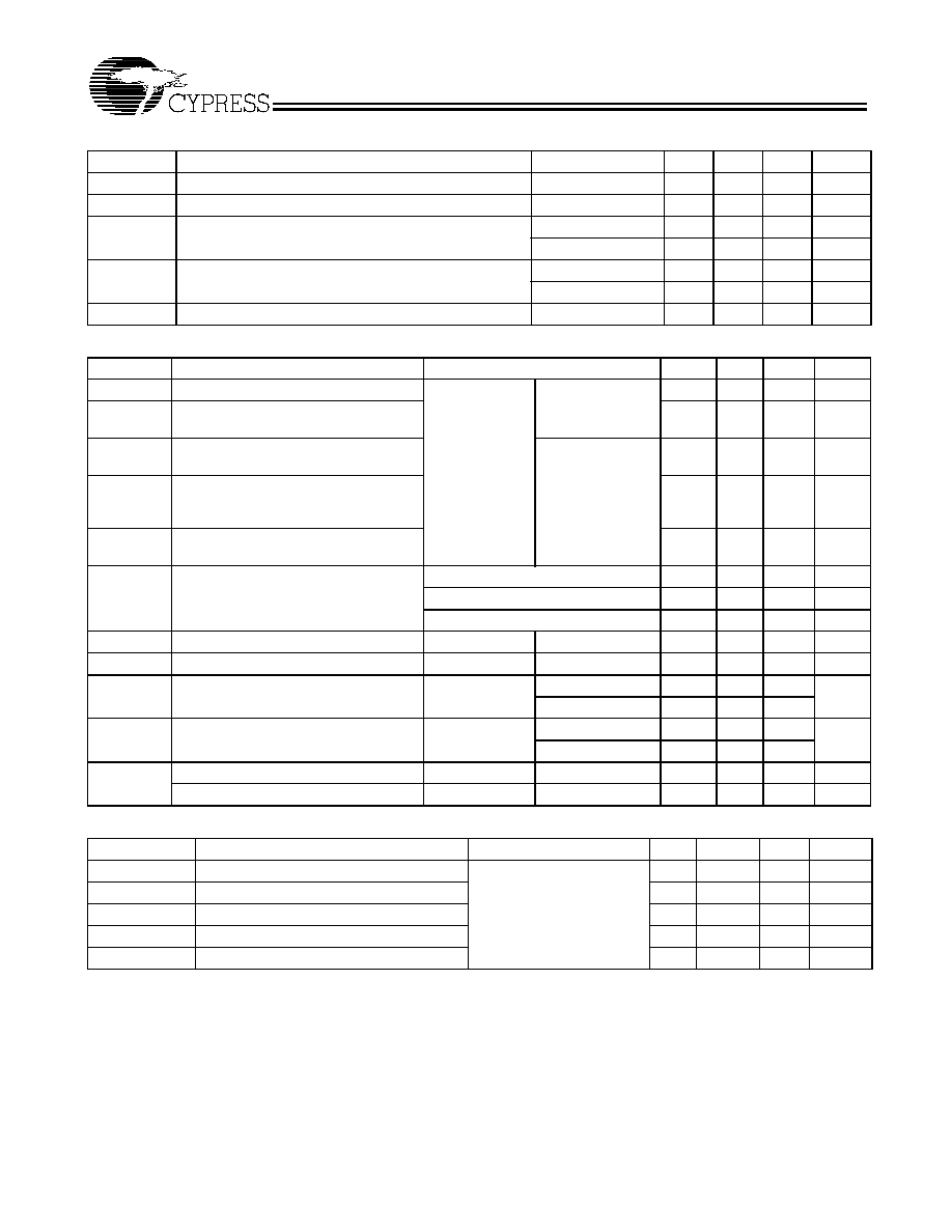
Table 4. Receiver Electrical Characteristics Over Recommended Operating Conditions
Parameter
Description
Test Conditions
Min.
Typ.
Max.
Unit
VITH+
Positive-going Differential Input Voltage Threshold
V
CM
= 1.2V
100
mV
VITH-
Negative-going Differential Input Voltage Threshold
V
CM
= 1.2V
100
mV
II
Input Current ( A Inputs)
VI = 0V
0.5
10
uA
VI = 2.4V
10
uA
II
Input Current (B Inputs)
VI = 0.8V
0.5
10
uA
VI = 2.4V
10
uA
II (Off)
Power Off Current (A or B Inputs)
V
DD
= 0V
0.1
10
uA
Table 5. Receiver Electrical Characteristics Over Recommended Operating Conditions
Parameter
Description
Test Conditions
Min.
Typ.
Max.
Unit
V
OD
Differential Output Voltage Swing
RL = 50 Ohm
See Figure 11,
Figures [15][19]
247
340
454
mV
~V
OD
Change in differential Output Voltage
Swing between logic states
-50
50
mV
V
OC
(SS)
Steady State Common-mode output
voltage
See Figure 12
1.125
1.375
V
~V
OC
(SS)
Change in Steady State
Common-mode output between logic
states
-50
3
50
mV
V
OC
(PP)
Peak to Peak Common-mode output
voltage
150
mV
I
CC
Supply Current
No load f = 100 MHz
30
mA
RL = 50 ohm, F = 100 MHz
35
mA
Both Channels Disabled
25
mA
I
H
High Level Input Current
S0,S1,DE
V
IH
= 5V
20
uA
I
IL
Low Level Input Current
S0,S1,DE
V
IL
= 0.8V
5
uA
I
OS
Short Circuit Current
V
OY
or V
0Z
= 0V
20
mA
V
OD
= 0V
20
I
OZ
High Impedance Output Current
V
OD
= 60mV
0.1
1
uA
V
O
= 0V or V
DD
0.1
1
C
in
Input Capacitance
1A, 1B, 2A, 2B
3
pF
Control Input Capacitance
S0, S1, 1DE, 2DE
8
pF
Table 6. Differential Receiver to Driver Switching Characteristics Over Recommended Operating Conditions
[[5]]
Parameter
Description
Test Conditions
Min.
Typ.
[[4]]
Max.
Unit
T
PLH
Differential Propagation delay, Low to High CL = 10 pF (see Figure 14)
4
6
nS
T
PHL
Differential Propagation delay, High to Low
4
6
nS
T
sk(p)
Pulse Skew ( T
PHL
T
PLH
)
0.2
nS
T
r
Transition Low to High
800
1500
pS
T
f
Transition High to Low
800
1500
pS
Notes:
4.
All typical values are measured at 25°C with a 3.3V supply.
5.
These parameters are measured over supply voltage and temperature ranges recommended for the device.
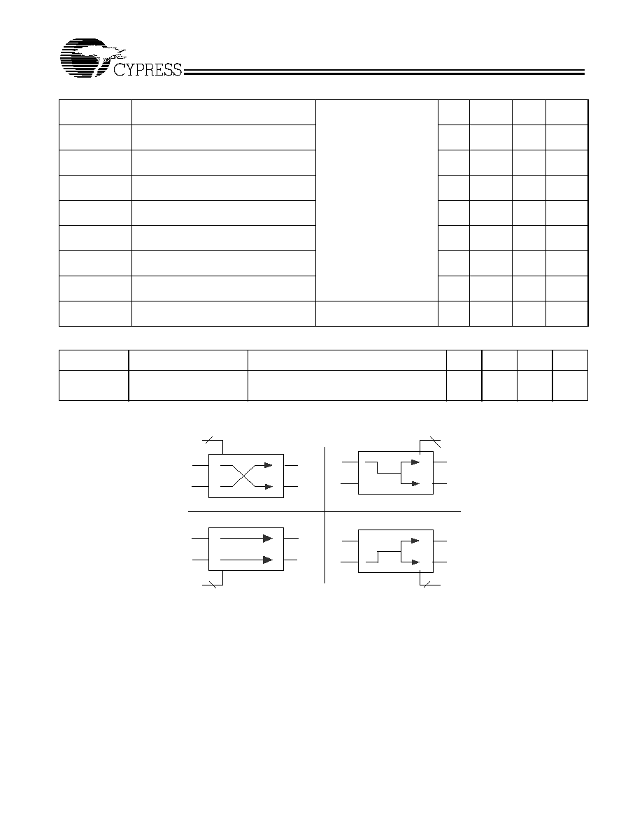
ComLinkTM Series
CY2LL843
Document #: 38-07066 Rev. *A
Page 4 of 13
T
PHZ
Propagation delay, High level to High
impedance output
(see Figure 14)
4
10
nS
T
PLZ
Propagation delay, Low level to High
impedance output
4.3
10
nS
T
PZH
Propagation delay, high impedance to High
level output
3
10
nS
T
PZL
Propagation delay, high impedance to Low
level output
2
10
nS
T
PHL_skR1_Dx
Channel to Channel skew-receiver 1 to Any
mux related drivers
95
pS
T
PLH_skR1_Dx
Channel to Channel skew-receiver 1 to Any
mux related drivers
95
pS
T
PPHL_skR2_Dx
Channel to Channel skew-receiver 2 to Any
mux related drivers
95
pS
T
PLH_skR2_Dx
Channel to Channel skew-receiver 2 to Any
mux related drivers
95
pS
D
J
Deterministic Jitter
(100MHz, 25°C,
VID =0.4V, S0, S1 = 0)
(see Figure 7)
PRBS-Differential
95
pS
Table 7. High Frequency Parametrics
Parameter
Description
Test Conditions
Min.
Typ.
Max.
Unit
F
max
Maximum frequency
V
DD
= 3.3V
50% duty cycle tW(5050)
Standard Load Circuit.
400
MHz
Table 6. Differential Receiver to Driver Switching Characteristics Over Recommended Operating Conditions (continued)
[[5]]
1A /1B
1Y/1Z
2Y/2Z
2A/2B
C ross
Point
R outer
1A/1B
2A/2B
2A /2B
1A/1B
1Y/1Z
2Y /2Z
Splitter A
1Y/1Z
2Y /2Z
Splitter B
S 0/S 1
S 0/S1
1A /1B
2A/2B
2Y/2Z
1Y/1Z
Pass
Thru
R outer
S 0/S 1
S 0/S1
Router O ptions
Splitter O ptions
Figure 1. Two-channel Cross Point Switch/Mux
ComLinkTM Series
CY2LL843
Document #: 38-07066 Rev. *A
Page 5 of 13
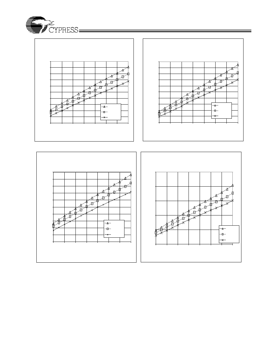
Dynamic IDD CY2LL843C
VID=0.4, VIC=1.2V S0, S1=00
Temp = 25°C
25.00
27.00
29.00
31.00
33.00
35.00
37.00
39.00
41.00
43.00
45.00
50
100
150
200
250
300
350
400
Fin (MHz)
I
dd (
m
A
)
Vdd=3.60V
Vdd=3.30V
Vdd=3.00V
Dynamic IDD CY2LL843C
VID=0.4, VIC=1.2V S0, S1=01
Temp = 25°C
25.00
27.00
29.00
31.00
33.00
35.00
37.00
39.00
41.00
43.00
45.00
50
100
150
200
250
300
350
400
Fin (MHz)
I
dd (mA
)
Vdd=3.60V
Vdd=3.30V
Vdd=3.00V
Figure 2. Dynamic IDD vs. Frequency 25 C
Dynamic IDD CY2LL843C
VID=0.4, VIC=1.2V S0, S1=00
Temp = 85°C
25.00
27.00
29.00
31.00
33.00
35.00
37.00
39.00
41.00
43.00
45.00
50
100
150
200
250
300
350
400
Fin (MHz)
I
dd (mA
)
Vdd=3.60V
Vdd=3.30V
Vdd=3.00V
Dynamic IDD CY2LL843C
VID=0.4, VIC=1.2V S0, S1=01
Temp = 85°C
25.00
30.00
35.00
40.00
45.00
50.00
50
100
150
200
250
300
350
400
Fin (MHz)
I
dd (
m
A
)
Vdd=3.60V
Vdd=3.30V
Vdd=3.00V
Figure 3. Dynamic IDD vs. Frequency 85 C