
PRELIMINARY
1.8V, 500-MHz, 10-Output JEDEC-Compliant
Zero Delay Buffer
CY2SSTU877
Cypress Semiconductor Corporation
∑
3901 North First Street
∑
San Jose
,
CA 95134
∑
408-943-2600
Document #: 38-07575 Rev. *B
Revised January 19, 2005
Features
∑ Operating frequency: 125 MHz to 500 MHz
∑ Supports DDRII SDRAM
∑ Ten differential outputs from one differential input
∑ Spread-Spectrum-compatible
∑ Low jitter (cycle-to-cycle): < 40 ps
∑ Very low skew: < 40 ps
∑ Power management control input
∑ 1.8V operation
∑ Fully JEDEC-compliant
∑ 52-ball BGA and a 40-pin MLF (QFN)
Functional Description
The CY2SSTU877 is a high-performance, low-skew, low-jitter
zero delay buffer designed to distribute differential clocks in
high-speed applications. The CY2SSTU877 generates ten
differential pair clock outputs from one differential pair clock
input. In addition, the CY2SSTU877 features differential
feedback clock outputs and inputs. This allows the
CY2SSTU877 to be used as a zero delay buffer. When used
as a zero delay buffer in nested clock trees, the CY2SSTU877
locks onto the input reference and translates with near zero
delay to low-skew outputs.
This phase-locked loop (PLL) clock buffer is designed for a
VDD of 1.8V, an AVDD of 1.8V and differential data input and
output levels. Package options include a plastic 52-ball
VFBGA and a 40-pin MLF (QFN). The device is a zero delay
buffer that distributes a differential clock input pair (CK, CK#)
to ten differential pair of clock outputs (Y[0:9], Y#[0:9]) and one
differential pair feedback clock outputs (FBOUT, FBOUT#).
The input clocks (CK, CK#), the feedback clocks (FBIN,
FBIN#), the LVCMOS (OE, OS), and the analog power input
(AVDD) control the clock outputs.
The PLL in the CY2SSTU877 clock driver uses the input
clocks (CK, CK#) and the feedback clocks (FBIN, FBIN#) to
provide high-performance, low-skew, low-jitter output differ-
ential clocks (Y[0:9], Y#[0:9]). The CY2SSTU877 is also able
to track Spread Spectrum Clocking (SSC) for reduced EMI.
When AVDD is grounded, the PLL is turned off and bypassed
for test purposes. When both clock signals (CK, CK#) are logic
low, the device will enter a low-power mode. An input logic
detection circuit on the differential inputs, independent from
the input buffers, will detect the logic low level and perform a
low-power state where all outputs, the feedback, and the PLL
are OFF. When the inputs transition from both being logic low
to being differential signals, the PLL will be turned back on, the
inputs and outputs will be enabled and the PLL will obtain
phase lock between the feedback clock pair (FBIN, FBIN#)
and the input clock pair (CK, CK#) within the specified stabili-
zation time t
L
.
Block Diagram
Pin Configuration
19
18
17
16
15
14
13
12
11
20
Y3
Y3
#
Y4
#
Y4
VD
D
Q
Y9
Y9
#
Y8
#
Y8
VD
D
Q
40 Q FN
C Y2S STU 877
30
29
28
27
26
25
24
23
22
21
Y7#
VD D Q
Y7
FB IN
FB IN #
FB O U T#
FB O U T
VD D Q
O E
O S
1
2
3
4
5
6
7
8
9
10
VD DQ
Y2
Y2#
C LK
C LK #
VD DQ
AG N D
A VD D
VD DQ
G N D
32
33
34
35
36
37
38
39
40
31
Y1#
Y1
Y0
Y0#
VDDQ
Y5#
Y5
Y6
Y6#
VDDQ
1
2
3
4
5
6
A
Y1
Y0
Y0#
Y5#
Y5
Y6
B
Y1#
GND
GND
GND
GND
Y6#
C
Y2#
GND
NB
NB
GND
Y7#
D
Y2
VDDQ
VDDQ
VDDQ
OS
Y7
E
CK
VDDQ
NB
NB
VDDQ
FBIN
F
CK#
VDDQ
NB
NB
OE
FBIN#
G
AGND
VDDQ
VDDQ
VDDQ
VDDQ
FBOUT#
H
AVDD
GND
NB
NB
GND
FBOUT
J
Y3
GND
GND
GND
GND
Y8
K
Y3#
Y4#
Y4
Y9
Y5#
Y8#
52 BGA
PRELIMINARY
CY2SSTU877
Document #: 38-07575 Rev. *B
Page 2 of 9
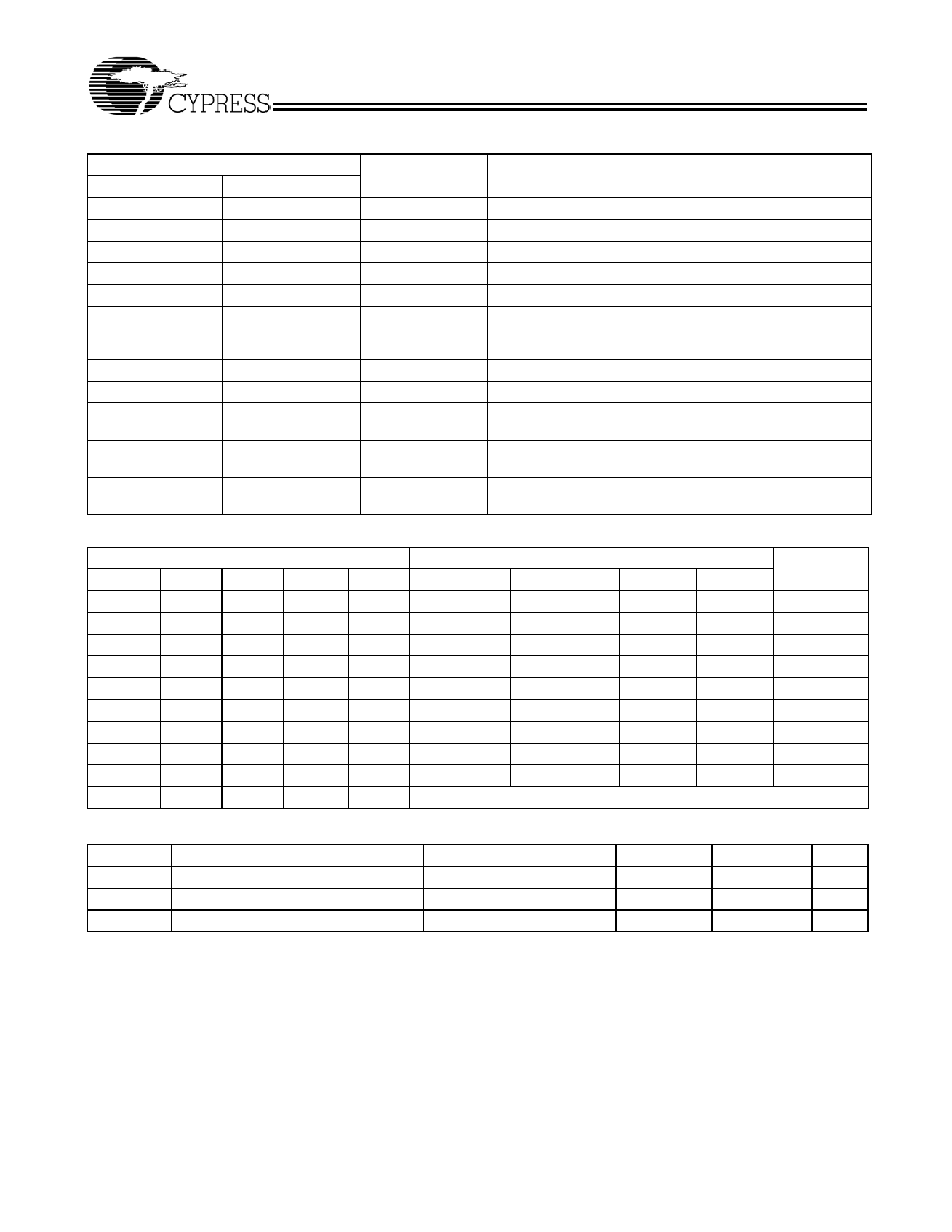
Pin Description
Pin No.
Name
Description
(BGA)
QFN
G1
7
AGND
Ground for 1.8V analog supply
H1
8
AVDD
1.8V analog supply
E1, F1
4, 5
CLK, CLK#
Differential clock input with a (10K≠100K
) pull-down resistor
E6, F6
27, 26
FBIN, FBIN#
Feedback differential clock input
H6, G6
24, 25
FBOUT, FBOUT#
Feedback differential clock output
B2, B3, B4, B5, C2,
C5, H2, H5, J2, J3,
J4, J5
10
GND
Ground
F5
22
OE
Output enable (ASYNC) for Y[0:9] and Y# [0:9]
D5
21
OS
Output Select (Tied to GND or VCC)
D2, D3, D4, E2, E5,
F2, G2, G3, G4, G5
1, 6, 9, 15, 20, 23, 28,
31, 36
VDDQ
1.8V supply
A2, A1, D1, J1, K3,
A5, A6, D6, J6, K4,
38, 39, 3, 11, 14, 34,
33, 29, 19, 16
Y [0:9]
Buffered output of input clock, CLK
A3, B1, C1, K1, K2,
A4, B6, C6, K6, K5
37, 40, 2, 12, 13, 35,
32, 30, 18, 17
Y# [0:9]
Buffered output of input clock, CLK
Table 1. Function Table
Inputs
Outputs
PLL
AVDD
OE
OS
CLK
CLK#
Y
Y#
FBOUT
FBOUT#
GND
H
X
L
H
L
H
L
H
Bypassed/Off
GND
H
X
H
L
H
L
H
L
Bypassed/Off
GND
L
H
L
H
Lz
Lz
L
H
Bypassed/Off
GND
L
L
H
L
Lz,Y7 Active
Lz,Y7# Active
H
L
Bypassed/Off
VDD
L
H
L
H
Lz
Lz
L
H
On
VDD
L
L
H
L
Lz,Y7 Active
Lz,Y7# Active
H
L
On
VDD
H
X
L
H
L
H
L
H
On
VDD
H
X
H
L
H
L
H
L
On
VDD
X
X
L
L
Lz
Lz
Lz
Lz
Off
X
X
X
H
H
Reserved
Recommended Operating Conditions
Parameter
Description
Condition
Min.
Max.
Unit
T
A
(Ind.)
Ambient Operating Temp
≠40
85
∞C
T
A
(Com.)
Ambient Operating Temp
0
70
∞C
V
DD
Operating Voltage
1.7
1.9
V

PRELIMINARY
CY2SSTU877
Document #: 38-07575 Rev. *B
Page 3 of 9
Absolute Maximum Conditions
Parameter
Description
Condition
Min.
Max.
Unit
V
IN
Input Voltage Range
≠0.5
V
DDQ
+ 0.5
V
V
OUT
Output Voltage Range
≠0.5
V
DDQ
+ 0.5
V
T
S
Storage Temperature
≠65
150
∞C
V
CC
Supply Voltage Range
≠0.5
2.5
V
I
IK
Input Clamp Current
≠50
50
mA
I
OK
Output Clamp Current
≠50
50
mA
I
O
Continuous Output Current
≠50
50
mA
Continuous Current through V
DD
/GND ≠100
100
mA
DC Electrical Specifications
Parameter
Description
Conditions
Min.
Max.
Unit
V
IX
Input Differential Crossing Voltage
(V
DDQ
/2) ≠ 0.15
(V
DDQ
/2) + 0.15
V
V
ID
DC
Input Differential Voltage (DC Values)
0.3
V
DDQ
+ 0.4
V
V
ID
AC
Input Differential Voltage (AC Values)
0.6
V
DDQ
+ 0.4
V
V
IL
Input Low Voltage
(OE, OS, CK, CK#)
0.35 * V
DDQ
V
V
IH
Input High Voltage
(OE, OS, CK, CK#)
0.65 * V
DDQ
V
V
OL
Output
Low
Voltage
I
OL
= 100
µA
0.1
V
I
OL
= 9 mA
0.6
V
V
OH
Output High Voltage
I
OH
= ≠100
µA
V
DDQ
≠ 0.2
V
I
OH
= ≠9 mA
1.1
V
I
OH
Output High Current
≠9
mA
I
OL
Output Low Current
9
mA
V
IK
Input Clamping Voltage
I
I
= ≠18 mA
≠1.2
V
V
OD
Output Differential Voltage
0.5
V
V
OX
Output Differential Crossing Voltage
V
DDQ
/2 ≠ 0.08
V
DDQ
/2 + 0.08
V
AC Electrical Specifications
Parameter
Description
Conditions
Min.
Max.
Unit
S
LR(O)
Output Slew Rate
Y[0:9], Y#[0:9], FBOUT,
FBOUT#
1.5
3
V/ns
S
LR(I)
Input Slew Rate
CLK, CLK#, FBIN, FBIN#
1
4
V/ns
OE
0.5
V/ns
C
IN
Input Capacitance
(Input Capacitance of CK, CK#,
FBIN, FBIN#) Vi = VDDQ or
GND
2
3
pF
C
OUT
pF
C
IN(DELTA)
Ci(delta) (CK, CK#, FBIN,
FBIN#) Vi = VDDQ or GND
≠0.25 0.25
pF
AC Timing Specifications
Parameter
Description
Conditions
Min.
Max.
Unit
F
CLK
Clock Frequency
125
500
MHz
T
DC
Duty Cycle
40
60
%
T
LOCK
PLL Lock Time
≠
10
µs
Tjitt (cc)
Cycle-to-cycle jitter
≠30
30
ps
Tjit (Period)
Period Cycle-to-cycle jitter
≠40
20
ps

