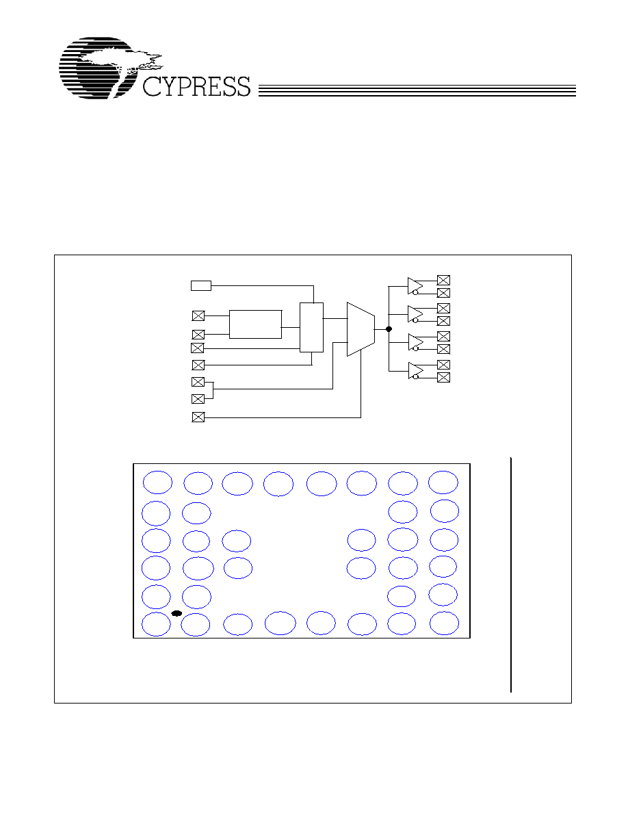
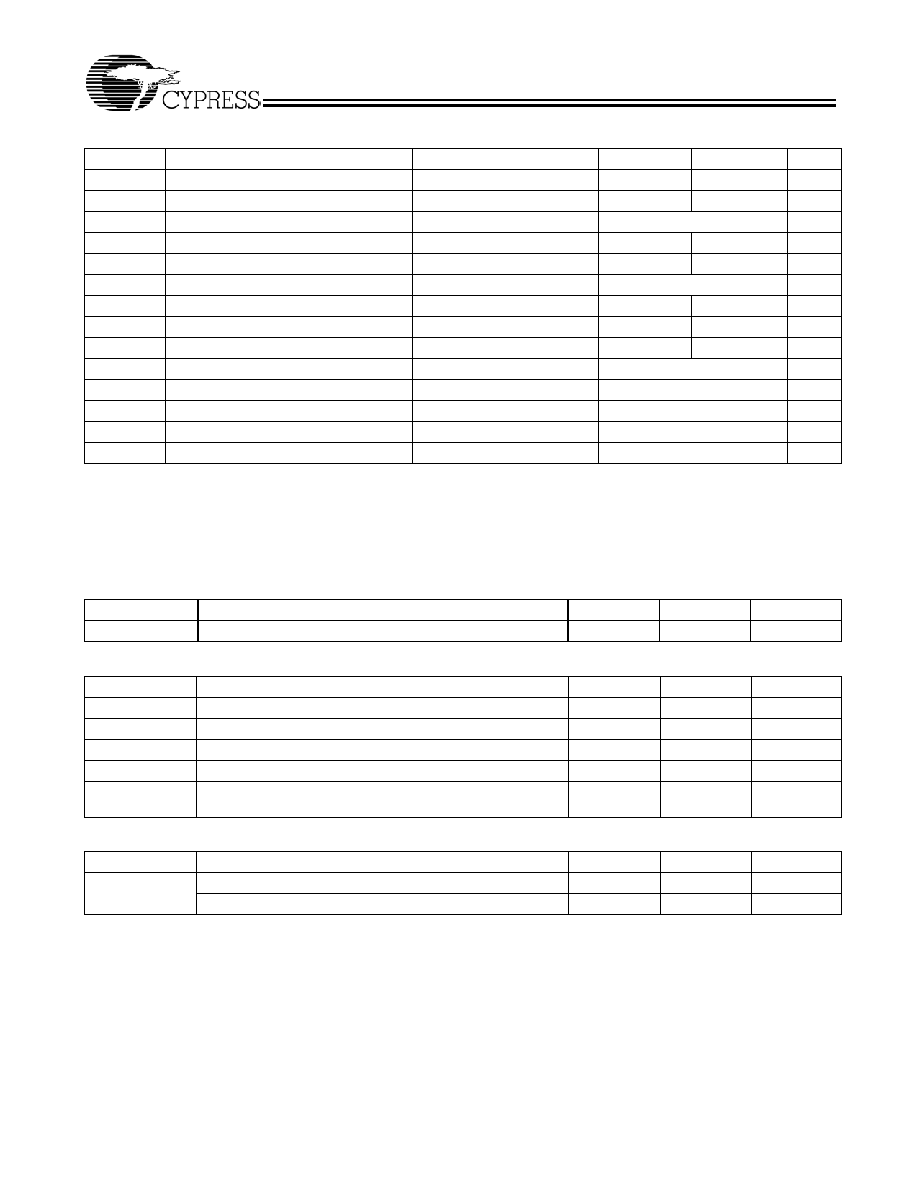
CY2XP304
Document #: 38-07589 Rev. *B
Page 2 of 11
CY2XP304 Two-Wire Serial Interface
Introduction
The CY2XP304 has a two-wire serial interface designed for
data transfer operations, and is used for programming the P
and Q values for frequency generation. S
clk
is the serial clock
line controlled by the master device. S
data
is a serial bidirec-
tional data line. The CY2XP304 is a slave device and can
either read or write information on the dataline upon request
from the master device.
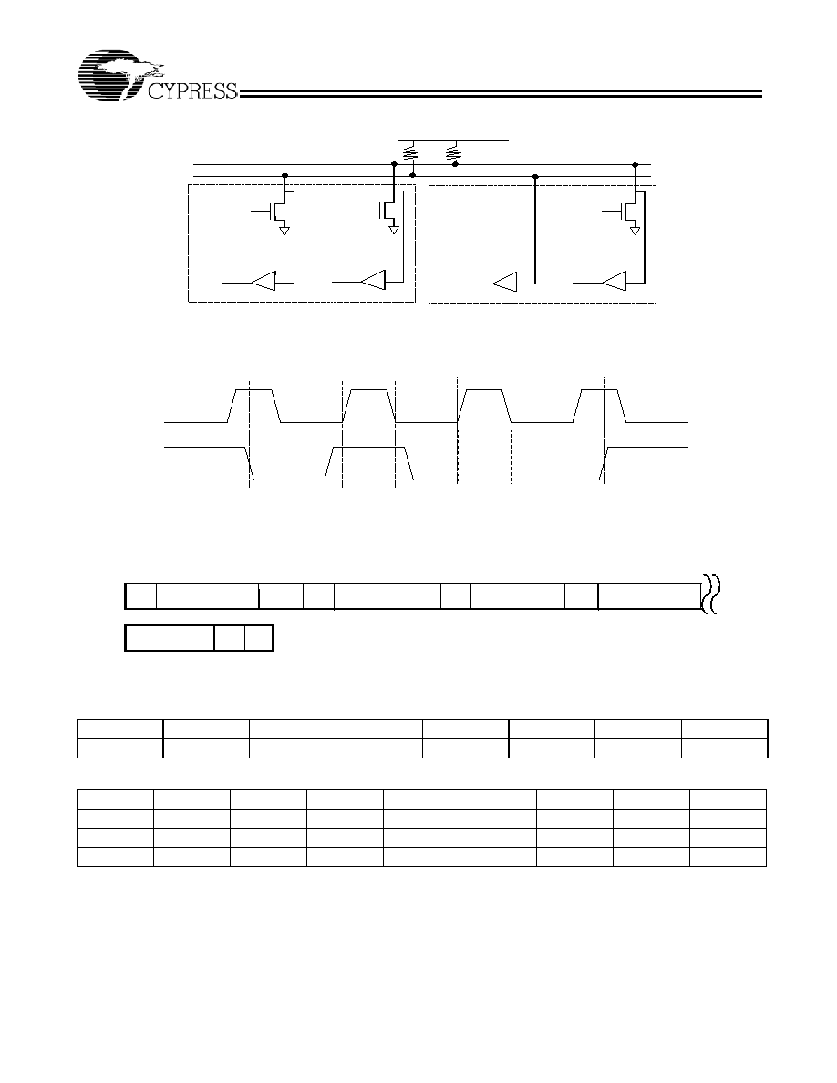
Figure 1 shows the basic bus connections between master
and slave device. The buses are shared by a number of
devices and are pulled HIGH by a pull-up resistor.
Serial Interface Specifications
Figure 2 shows the basic transmission specification. To begin
and end a transmission, the master device generates a start
signal (S) and a stop signal (P). Start (S) is defined as
switching the S
data
from HIGH to LOW while the S
clk
is at
HIGH. Similarly, stop (P) is defined as switching the S
data
from
LOW to HIGH while holding the S
clk
HIGH. Between these two
signals, data on S
data
is synchronous with the clock on the S
clk
.
Data is allowed to change only at LOW period of clock, and
must be stable at the HIGH period of clock. To acknowledge,
drive the S
data
LOW before the S
clk
rising edge and hold it
LOW until the S
clk
falling edge.
Serial Interface Format
Each slave carries an address. The data transfer is initiated by
a start signal (S). Each transfer segment is one byte in length.
The slave address and the read/write bit are first sent from the
master device after the start signal. The addressed slave
device must acknowledge (Ack) the master device. Depending
on the Read/Write bit, the master device will either write data
into (logic 0) or read data (logic 1) from the slave device. Each
time a byte of data is successfully transferred, the receiving
device must acknowledge. At the end of the transfer, the
master device will generate a stop signal (P).
Serial Interface Transfer Format
Figure 2 shows the serial interface transfer format used with
the CY2XP304. Two dummy bytes must be transferred before
the first data byte. The CY2XP304 has only three bytes of
latches to store information, and the third byte of data is
reserved. Extra data will be ignored.
Pin Definitions
Pin #
Pin Name
Pin Description
A1,B1,G3,G4
VDDB
3.3V Power Supply for Crystal Driver
A2
XIN
Reference Crystal Input
A3
XOUT
Reference Crystal Feedback
A4,B2,C1,C3,C4,F3,F4,G2,G5,B5
GND
Ground
A5,H1,H2,H4,H5
VDDA
3.3V Power Supply
A6
CLK0
LVPECL Clock Output
B6
CLK0B
LVPECL Clock Output (Complement)
C6
CLK1
LVPECL Clock Output
D6
CLK1B
LVPECL Clock Output (Complement)
E6
CLK2
LVPECL Clock Output
F6
CLK2B
LVPECL Clock Output (Complement)
G6
CLK3
LVPECL Clock Output
H6
CLK3B
LVPECL Clock Output (Complement)
B3
SER_CLK Serial Interface Clock
B4
SER_DATA Serial Interface Data
D1
PLL_MULT PLL Multiplier Select Input, Internal pull-up resistor, see Frequency Table
E1
CLK_SEL Clock Select Input, Internal Pull down. HIGH select INA/INAB, Internal PLL
is bypassed. LOW select internal PLL
F1,G1
INA,INAB Differential Clock Input pair, used in PLL-bypassed mode
H3
NC
No Connect
Frequency Table
PLL_Mult
M (PLL Multiplier)
Example Input Crystal Frequency
CLK[0:3],CLKB[0:3]
0
x16
25 MHz
400 MHz
31.25 MHz
500 MHz
1
x8
15.625 MHz
125 MHz
CY2XP304
Document #: 38-07589 Rev. *B
Page 3 of 11
To program the CY2XP304 using the two-wire serial interface,
set the SELPQ bit HIGH. The default setting of this bit is LOW.
The P and Q values are determined by the following formulas:
P
final
= (P
7..0
+ 3) * 2
Q
final
= Q
5..0
+ 2
If the QCNTBYP bit is set HIGH, then Q
final
defaults to a value
of 1. The default setting of this bit is LOW.
If the SELPQ bit is set LOW, the PLL multipliers will be set
using the values in the Select Function Table.
CyberClocksTM has been developed to generate P and Q
values for stable PLL operation. This software is downloadable
from www.cypress.com.
Figure 1. Device Connections
Figure 2. Serial Interface Specifications
Figure 3. CY2XP304 Transfer Format
Serial Interface Address for the CY2XP304
A6
A5
A4
A3
A2
A1
A0
R/W
1
1
0
0
1
0
1
0
Serial Interface Programming for the CY2XP304
b7
b6
b5
b4
b3
b2
b1
b0
Data0
QCNTBYP
SELPQ
Q<5>
Q<4>
Q<3>
Q<2>
Q<1>
Q<0>
Data1
P<7>
P<6>
P<5>
P<4>
P<3>
P<2>
P<1>
P<0>
Data2
Reserved
Reserved
Reserved
Reserved
Reserved
Reserved
Reserved
Reserved
S
clk
S
da ta
S
clk
_C
S
clk
_in
S
data
_C
S
data
_in
M a ste r D e vice
R
p
S
clk
_in
S
data
_C
S
data
_in
S lave D evice
V
D D
R
p
Start (S)
Stop (P)
S
clk
S
data
valid data
Acknowledge
Ack
1 bit
8 bits
Data 1
P
Slave Address
Ack
S
Dummy Byte 0
R/W
Dummy Byte 1
Ack
1 bit
1 bit
Ack
1 bit
7 bits
8 bits
1 bit
Data 0
Ack
1 bit
8 bits
1 bit
8 bits
CY2XP304
Document #: 38-07589 Rev. *B
Page 4 of 11
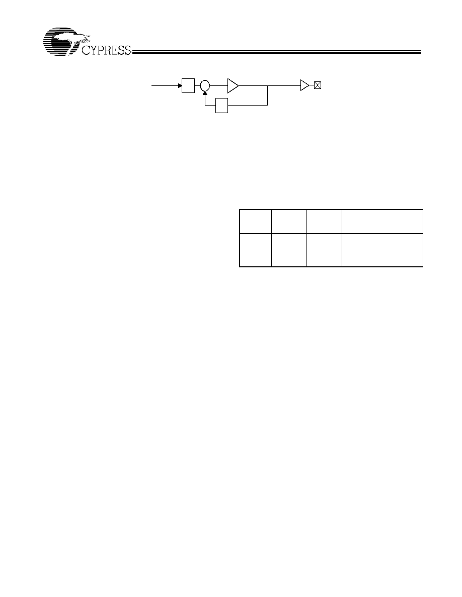
PLL Frequency = Reference x P/Q = Output
Functional Specifications
Crystal Input
The CY2XP304 receives its reference from an external crystal.
Pin XIN is the reference crystal input, and pin XOUT is the
reference crystal feedback. The parameters for the crystal are
given on page 5 of this data sheet. The oscillator circuit
requires external capacitors. Please refer to the application
note entitled Crystal Oscillator Topics for details.
Select Input
There are two select input pins, the PLL_MULT and CLK_SEL.
PLL_MULT pin selects the frequency multiplier in the PLL, and
is a standard LVCMOS input. The S pin has an internal pull-up
resistor. The multiplier selection is given on page 2 of this data
sheet (see Frequency Table).
State Transition Characteristics
Specifies the maximum settling time of the CLK and CLKB
outputs from device power-up. For V
DD
and V
DDX
any
sequences are allowed to power-up and power-down the
CY2XP304.
Reference
PLL
Q
P
VCO
Output
Figure 4. PLL Block Diagram
State Transition Characteristics
From
To
Transi-
tion La-
tency
Description
V
DD
/V
DD
X
On
CLK/CLK
B Normal
3 ms
Time from V
DD
/V
DDX
is
applied and settled to
CLK/CLKB outputs
settled.
CY2XP304
Document #: 38-07589 Rev. *B
Page 5 of 11
Crystal Requirements
Requirements to use parallel mode fundamental xtal. External
capacitors are required in the crystal oscillator circuit. Please
refer to the application note entitled Crystal Oscillator Topics
for details.
Note:
1. Where V
CC
is 3.3V±5%
Absolute Maximum Conditions
Parameter
Description
Condition
Min.
Max.
Unit
V
CC
Supply Voltage
Non-functional
0.3
4.6
V
V
CC
Operating Voltage
Functional
3.135
3.465
V
VTT
Output Termination Voltage
Relative to V
CC
[1]
V
CC
2
V
V
IN
Input Voltage
Relative to V
CC
[1]
0.3
V
CC
+ 0.3
V
V
OUT
Output Voltage
Relative to V
CC
[1]
0.3
V
CC
+ 0.3
V
LU
I
Latch Up Immunity
Functional
100
mA
T
S
Temperature, Storage
Non-functional
65
+150
°C
T
A
Temperature, Operating Ambient
Functional
40
+85
°C
T
J
Temperature, Junction
Non-functional
150
°C
Ø
Jc
Dissipation, Junction to Case
Functional
11.38
°C/W
Ø
Ja
Dissipation, Junction to Ambient
Functional
85.83
°C/W
ESD
h
ESD Protection (Human Body Model)
2000
V
M
SL
Moisture Sensitivity Level
3
N.A.
G
ATES
Total Functional Gate Count
Assembled die
50
Ea.
Crystal Requirements
Parameter
Description
Min.
Max.
Unit
X
F
Frequency
10
31.25
MHz
DC Electrical Specifications
Parameter
Description
Min.
Max.
Unit
V
DD
Supply voltage
3.135
3.465
V
V
IL
Input signal low voltage at pin PLL_MULT
0.35
V
V
IH
Input signal high voltage at pin PLL_MULT
0.65
V
R
PUP
Internal pull-up resistance
10
100
k
t
PU
Power-up time for all V
DD
s to reach minimum specified voltage
(power ramps must be monotonic)
0.05
500
ms
Operating Conditions
Parameter
Description
Min.
Max.
Unit
T
A
Commercial Temperature
0
70
°C
Industrial Temperature
40
85
°C