128K x 36 Synchronous-Pipelined Cache RAM
CY7C1347B
Cypress Semiconductor Corporation
·
3901 North First Street
·
San Jose
·
CA 95134
·
408-943-2600
March 11, 2001
1CY7C1347
Features
· Supports 100-MHz bus for Pentium
and PowerPCTM
operations with zero wait states
· Fully registered inputs and outputs for pipelined oper-
ation
· 128K by 36 common I/O architecture
· 3.3V core power supply
· 2.5V/3.3V I/O operation
· Fast clock-to-output times
-- 3.5 ns (for 166-MHz device)
-- 4.0 ns (for 133-MHz device)
-- 5.5 ns (for 100-MHz device)
· User-selectable burst counter supporting Intel
Pen-
tium interleaved or linear burst sequences
· Separate processor and controller address strobes
· Synchronous self-timed writes
· Asynchronous output enable
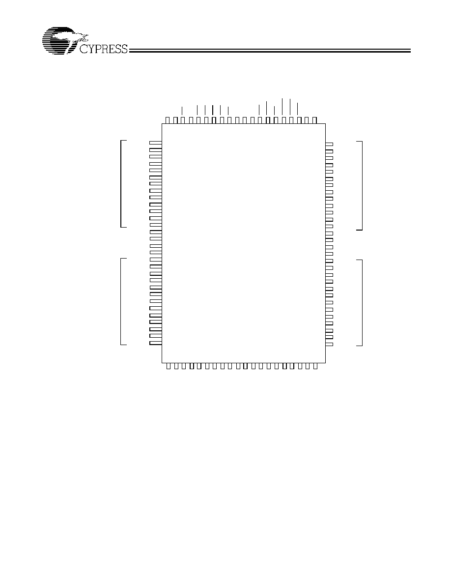
· JEDEC-standard 100 TQFP pinout
· "ZZ" Sleep Mode option and Stop Clock option
· Available in Industrial and Commercial Temperature
ranges
Functional Description
The CY7C1347B is a 3.3V, 128K by 36 synchronous-pipelined
cache SRAM designed to support zero-wait-state secondary
cache with minimal glue logic.
The CY7C1347B I/O pins can operate at either the 2.5V or the
3.3V level, the I/O pins are 3.3V tolerant when V
DDQ
= 2.5V.
All synchronous inputs pass through input registers controlled
by the rising edge of the clock. All data outputs pass through
output registers controlled by the rising edge of the clock. Max-
imum access delay from the clock rise is 3.5 ns (166-MHz
device).
The CY7C1347B supports either the interleaved burst se-
quence used by the Intel Pentium processor or a linear burst
sequence used by processors such as the PowerPC. The burst
sequence is selected through the MODE pin. Accesses can be
initiated by asserting either the Processor Address Strobe
(ADSP) or the Controller Address Strobe (ADSC) at clock rise.
Address advancement through the burst sequence is con-
trolled by the ADV input. A 2-bit on-chip wraparound burst
counter captures the first address in a burst sequence and
automatically increments the address for the rest of the burst
access.
Byte write operations are qualified with the four Byte Write
Select (BW
[3:0]
) inputs. A Global Write Enable (GW) overrides
all byte write inputs and writes data to all four bytes. All writes
are conducted with on-chip synchronous self-timed write cir-
cuitry.
Three synchronous Chip Selects (CE
1
, CE
2
, CE
3
) and an
asynchronous Output Enable (OE) provide for easy bank se-
lection and output three-state control. In order to provide prop-
er data during depth expansion, OE is masked during the first
clock of a read cycle when emerging from a deselected state.
Pentium and Intel are registered trademarks of Intel Corporation.
PowerPC is a trademark of IBM Corporation.
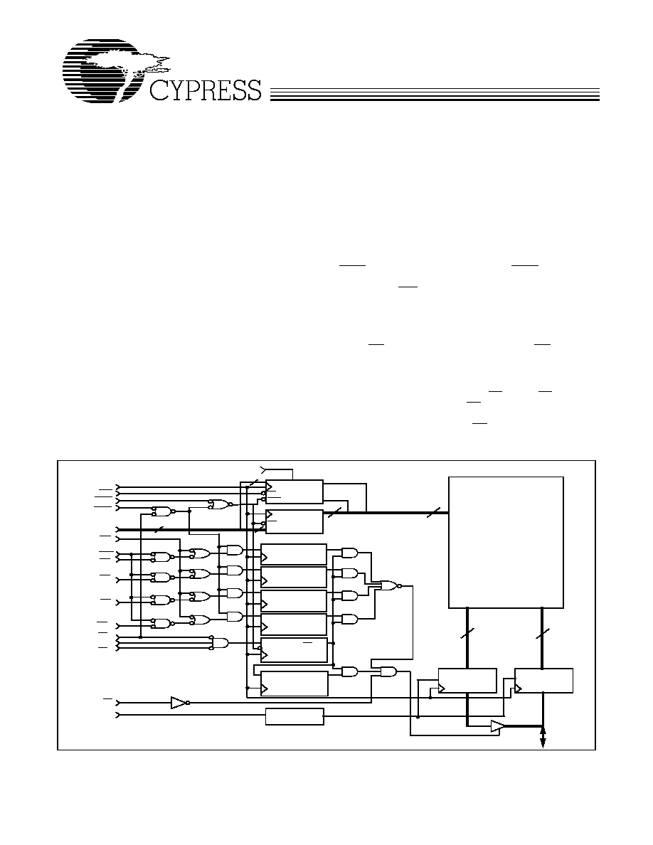
CLK
ADV
ADSC
A
[16:0]
GW
BWE
BW
3
BW
2
BW
1
BW
0
CE
1
CE
3
CE
2
OE
ZZ
BURST
COUNTER
ADDRESS
REGISTER
OUTPUT
REGISTERS
INPUT
REGISTERS
128KX36
MEMORY
ARRAY
CLK
CLK
Q
0
Q
1
Q
D
CE
CE
CLR
SLEEP
CONTROL
36
36
17
15
15
17
(A
[1;0]
)
2
MODE
ADSP
Logic Block Diagram
DQ
[31:0]
DP
[3:0]
DQ[31:24], DP[3]
BYTEWRITE
REGISTERS
D
Q
DQ[23:16], DP[2]
BYTEWRITE
REGISTERS
D
Q
D
Q
DQ[15:8], DP[1]
BYTEWRITE
REGISTERS
DQ[7:0], DP[0]
BYTEWRITE
REGISTERS
D
Q
ENABLE CE
REGISTER
D
Q
ENABLE DELAY
REGISTER
D
Q
CY7C1347B
4
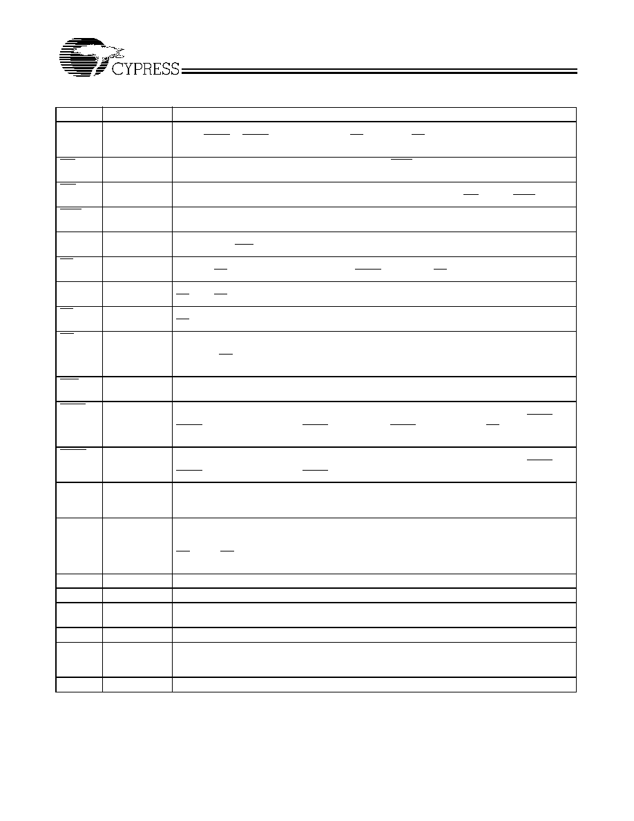
Pin Definitions
Name
I/O
Description
A
[16:0]
Input-
Synchronous
Address Inputs used to select one of the 64K address locations. Sampled at the rising edge of the
CLK if ADSP or ADSC is active LOW, and CE
1
,
CE
2
, and
CE
3
are sampled active. A
[1:0]
feed the
2-bit counter.
BW
[3:0]
Input-
Synchronous
Byte Write Select Inputs, active LOW. Qualified with BWE to conduct byte writes to the SRAM.
Sampled on the rising edge of CLK.
GW
Input-
Synchronous
Global Write Enable Input, active LOW. When asserted LOW on the rising edge of CLK, a global
write is conducted (ALL bytes are written, regardless of the values on BW
[3:0]
and BWE).
BWE
Input-
Synchronous
Byte Write Enable Input, active LOW. Sampled on the rising edge of CLK. This signal must be
asserted LOW to conduct a byte write.
CLK
Input-Clock
Clock Input. Used to capture all synchronous inputs to the device. Also used to increment the burst
counter when ADV is asserted LOW, during a burst operation.
CE
1
Input-
Synchronous
Chip Enable 1 Input, active LOW. Sampled on the rising edge of CLK. Used in conjunction with
CE
2
and CE
3
to select/deselect the device. ADSP is ignored if CE
1
is HIGH.
CE
2
Input-
Synchronous
Chip Enable 2 Input, active HIGH. Sampled on the rising edge of CLK. Used in conjunction with
CE
1
and CE
3
to select/deselect the device.
CE
3
Input-
Synchronous
Chip Enable 3 Input, active LOW. Sampled on the rising edge of CLK. Used in conjunction with
CE
1
and
CE
2
to select/deselect the device.
OE
Input-
Asynchronous
Output Enable, asynchronous input, active LOW. Controls the direction of the I/O pins. When LOW,
the I/O pins behave as outputs. When deasserted HIGH, I/O pins are three-stated, and act as input
data pins. OE is masked during the first clock of a read cycle when emerging from a deselected
state.
ADV
Input-
Synchronous
Advance Input signal, sampled on the rising edge of CLK. When asserted, it automatically incre-
ments the address in a burst cycle.
ADSP
Input-
Synchronous
Address Strobe from Processor, sampled on the rising edge of CLK. When asserted LOW, A
[16:0]
is captured in the address registers. A
[1:0]
are also loaded into the burst counter. When ADSP and
ADSC are both asserted, only ADSP is recognized. ASDP is ignored when CE
1
is deasserted
HIGH.
ADSC
Input-
Synchronous
Address Strobe from Controller, sampled on the rising edge of CLK. When asserted LOW, A
[16:0]
is captured in the address registers. A
[1:0]
are also loaded into the burst counter. When ADSP and
ADSC are both asserted, only ADSP is recognized.
ZZ
Input-
Asynchronous
ZZ "sleep" Input. This active HIGH input places the device in a non-time-critical "sleep" condition
with data integrity preserved. For normal operation, this pin has to be LOW or left floating. ZZ pin
has an internal pull-down.
DQ
[31:0]
DP
[3:0]
I/O-
Synchronous
Bidirectional Data I/O lines. As inputs, they feed into an on-chip data register that is triggered by
the rising edge of CLK. As outputs, they deliver the data contained in the memory location specified
by A
[16:0]
during the previous clock rise of the read cycle. The direction of the pins is controlled by
OE. When OE is asserted LOW, the pins behave as outputs. When HIGH, DQ
[31:0]
and DP
[3:0]
are
placed in a three-state condition.
V
DD
Power Supply
Power supply inputs to the core of the device. Should be connected to 3.3V power supply.
V
SS
Ground
Ground for the core of the device. Should be connected to ground of the system.
V
DDQ
I/O Power
Supply
Power supply for the I/O circuitry. Should be connected to a 3.3V or 2.5V power supply.
V
SSQ
I/O Ground
Ground for the I/O circuitry. Should be connected to ground of the system.
MODE
Input-
Static
Selects Burst Order. When tied to GND selects linear burst sequence. When tied to V
DDQ
or left
floating selects interleaved burst sequence. This is a strap pin and should remain static during
device operation. Mode Pin has an internal pull-up.
NC
No Connects.

CY7C1347B
5
Introduction
Functional Overview
All synchronous inputs pass through input registers controlled
by the rising edge of the clock. All data outputs pass through
output registers controlled by the rising edge of the clock.
Maximum access delay from the clock rise (t
CO
) is 3.5 ns
(166-MHz device).
The CY7C1347B supports secondary cache in systems utiliz-
ing either a linear or interleaved burst sequence. The inter-
leaved burst order supports Pentium and i486 processors. The
linear burst sequence is suited for processors that utilize a
linear burst sequence. The burst order is user selectable, and
is determined by sampling the MODE input. Accesses can be
initiated with either the Processor Address Strobe (ADSP) or
the Controller Address Strobe (ADSC). Address advancement
through the burst sequence is controlled by the ADV input. A
two-bit on-chip wraparound burst counter captures the first ad-
dress in a burst sequence and automatically increments the
address for the rest of the burst access.
Byte write operations are qualified with the Byte Write Enable
(BWE) and Byte Write Select (BW
[3:0]
) inputs. A Global Write
Enable (GW) overrides all byte write inputs and writes data to
all four bytes. All writes are simplified with on-chip synchro-
nous self-timed write circuitry.
Three synchronous Chip Selects (CE
1
, CE
2
, CE
3
) and an
asynchronous Output Enable (OE) provide for easy bank se-
lection and output three-state control. ADSP is ignored if CE
1
is HIGH.
Single Read Accesses
This access is initiated when the following conditions are sat-
isfied at clock rise: (1) ADSP or ADSC is asserted LOW, (2)
CE
1
, CE
2
, CE
3
are all asserted active, and (3) the write signals
(GW, BWE) are all deasserted HIGH. ADSP is ignored if CE
1
is HIGH. The address presented to the address inputs (A
[16:0]
)
is stored into the address advancement logic and the Address
Register while being presented to the memory core. The cor-
responding data is allowed to propagate to the input of the
Output Registers. At the rising edge of the next clock the data
is allowed to propagate through the Output Register and onto
the data bus within 3.5 ns (166-MHz device) if OE is active
LOW. The only exception occurs when the SRAM is emerging
from a deselected state to a selected state, its outputs are
always three-stated during the first cycle of the access. After
the first cycle of the access, the outputs are controlled by the
OE signal. Consecutive single read cycles are supported.
Once the SRAM is deselected at clock rise by the chip select
and either ADSP or ADSC signals, its output will three-state
immediately.
Single Write Accesses Initiated by ADSP
This access is initiated when both of the following conditions
are satisfied at clock rise: (1) ADSP is asserted LOW, and (2)
CE
1
, CE
2
, CE
3
are all asserted active. The address presented
to A
[16:0]
is loaded into the Address Register and the address
advancement logic while being delivered to the RAM core. The
write signals (GW, BWE, and BW
[3:0]
) and ADV inputs are ig-
nored during this first cycle.
ADSP-triggered write accesses require two clock cycles to
complete. If GW is asserted LOW on the second clock rise, the
data presented to the DQ
[31:0]
and DP
[3:0]
inputs is written into
the corresponding address location in the RAM core. If GW is
HIGH, then the write operation is controlled by BWE and
BW
[3:0]
signals. The CY7C1347B provides byte write capabil-
ity that is described in the Write Cycle Description table. As-
serting the Byte Write Enable input (BWE) with the selected
Byte Write (BW
[3:0]
) input will selectively write to only the de-
sired bytes.
Bytes not selected during a byte write operation will remain
unaltered. A synchronous self-timed write mechanism has
been provided to simplify the write operations.
Because the CY7C1347B is a common I/O device, the Output
Enable (OE) must be deasserted HIGH before presenting data
to the DQ
[31:0]
and DP
[3:0]
inputs. Doing so will three-state the
output drivers. As a safety precaution, DQ
[31:0]
and DP
[3:0]
are
automatically three-stated whenever a write cycle is detected,
regardless of the state of OE.
Single Write Accesses Initiated by ADSC
ADSC write accesses are initiated when the following condi-
tions are satisfied: (1) ADSC is asserted LOW, (2) ADSP is
deasserted HIGH, (3) CE
1
, CE
2
, CE
3
are all asserted active,
and (4) the appropriate combination of the write inputs (GW,
BWE, and BW
[3:0]
) are asserted active to conduct a write to
the desired byte(s). ADSC-triggered write accesses require a
single clock cycle to complete. The address presented to
A
[16:0]
is loaded into the address register and the address ad-
vancement logic while being delivered to the RAM core. The
ADV input is ignored during this cycle. If a global write is con-
ducted, the data presented to the DQ
[31:0]
and DP
[3:0]
is written
into the corresponding address location in the RAM core. If a
byte write is conducted, only the selected bytes are written.
Bytes not selected during a byte write operation will remain
unaltered. A synchronous self-timed write mechanism has
been provided to simplify the write operations.
Because the CY7C1347B is a common I/O device, the Output
Enable (OE) must be deasserted HIGH before presenting data
to the DQ
[31:0]
and DP
[3:0]
inputs. Doing so will three-state the
output drivers. As a safety precaution, DQ
[31:0]
and DP
[3:0]
are
automatically three-stated whenever a write cycle is detected,
regardless of the state of OE.
Burst Sequences
The CY7C1347B provides a two-bit wraparound counter, fed
by A
[1:0]
, that implements either an interleaved or linear burst
sequence. The interleaved burst sequence is designed specif-
ically to support Intel Pentium applications. The linear burst
sequence is designed to support processors that follow a lin-
ear burst sequence. The burst sequence is user-selectable
through the MODE input.
Asserting ADV LOW at clock rise will automatically increment
the burst counter to the next address in the burst sequence.
Both read and write burst operations are supported.