/home/web/doc/html/cypress/169494
PRELIMINARY
128Kx36 Flow-Through SRAM with NoBLTM Architecture
CY7C1351B
Cypress Semiconductor Corporation
·
3901 North First Street
·
San Jose, CA 95134
·
408-943-2600
Document #: 38-05208 Rev. *A
Revised November 19, 2002
351B
Features
· Pin compatible and functionally equivalent to ZBTTM de-
vices IDT71V547, MT55L128L36F, and MCM63Z737
· Supports 66-MHz bus operations with zero wait states
-- Data is transferred on every clock
· Internally self-timed output buffer control to eliminate
the need to use OE
· Registered inputs for Flow-Through operation
· Byte Write capability
· 128K x 36 common I/O architecture
· Single 3.3V power supply
· Fast clock-to-output times
-- 7.5 ns (for 117-MHz device)
-- 8.5 ns (for 100-MHz device)
-- 11.0 ns (for 66-MHz device)
-- 12.0 ns (for 50-MHz device)
-- 14.0 ns (for 40-MHz device)
· Clock Enable (CEN) pin to suspend operation
· Synchronous self-timed writes
· Asynchronous Output Enable
· Standard 100 TQFP and 119 BGA packages
· Burst Capability--linear or interleaved burst order
Low standby power
Functional Description
The CY7C1351B is a 3.3V, 128K by 36 Synchronous
Flow-Through Burst SRAM designed specifically to support
unlimited true back-to-back Read/Write operations without the
insertion of wait states. The CY7C1351B is equipped with the
advanced No Bus LatencyTM (NoBLTM) logic required to en-
able consecutive Read/Write operations with data being trans-
ferred on every clock cycle. This feature dramatically improves
the throughput of data through the SRAM, especially in sys-
tems that require frequent Write/Read transitions. The
CY7C1351B is pin/functionally compatible to ZBT SRAMs
IDT71V547, MT55L128L36F, and MCM63Z737.
All synchronous inputs pass through input registers controlled
by the rising edge of the clock.The clock input is qualified by
the Clock Enable (CEN) signal, which, when deasserted, sus-
pends operation and extends the previous clock cycle. Maxi-
mum access delay from the clock rise is 7.5 ns (117-MHz
device).
Write operations are controlled by the four Byte Write Select
(BWS
[3:0]
) and a Write Enable (WE) input. All writes are con-
ducted with on-chip synchronous self-timed write circuitry.
Three synchronous Chip Enables (CE
1
, CE
2
, CE
3
) and an
asynchronous Output Enable (OE) provide for easy bank se-
lection and output three-state control. In order to avoid bus
contention, the output drivers are synchronously three-stated
during the data portion of a write sequence.
.
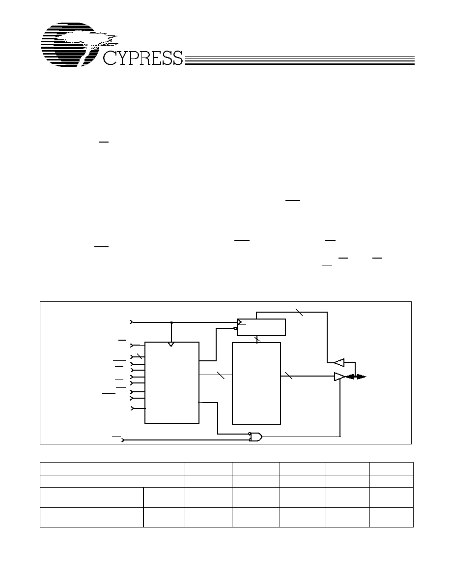
CLK
A
[16:0]
CEN
WE
BWS
CE
1
CE
3
CE
2
OE
128KX36
MEMORY
ARRAY
Logic Block Diagram
DQ
[31:0]
Data-In REG.
Q
D
CE
CONTROL
and WRITE
LOGIC
[3:0]
ADV/LD
36
36
17
17
36
Mode
DP
[3:0]
Selection Guide
7C1351B-117
7C1351B-100
7C1351B-66
7C1351B-50
7C1351B-40
Maximum Access Time (ns)
7.5
8.5
11.0
12.0
14.0
Maximum Operating Current
(mA)
Commercial
375 mA
350 mA
250 mA
200 mA
175 mA
Maximum CMOS Standby
Current (mA)
Commercial
5 mA
5 mA
5 mA
5 mA
5 mA
CY7C1351B
PRELIMINARY
Document #: 38-05208 Rev. *A
Page 2 of 16
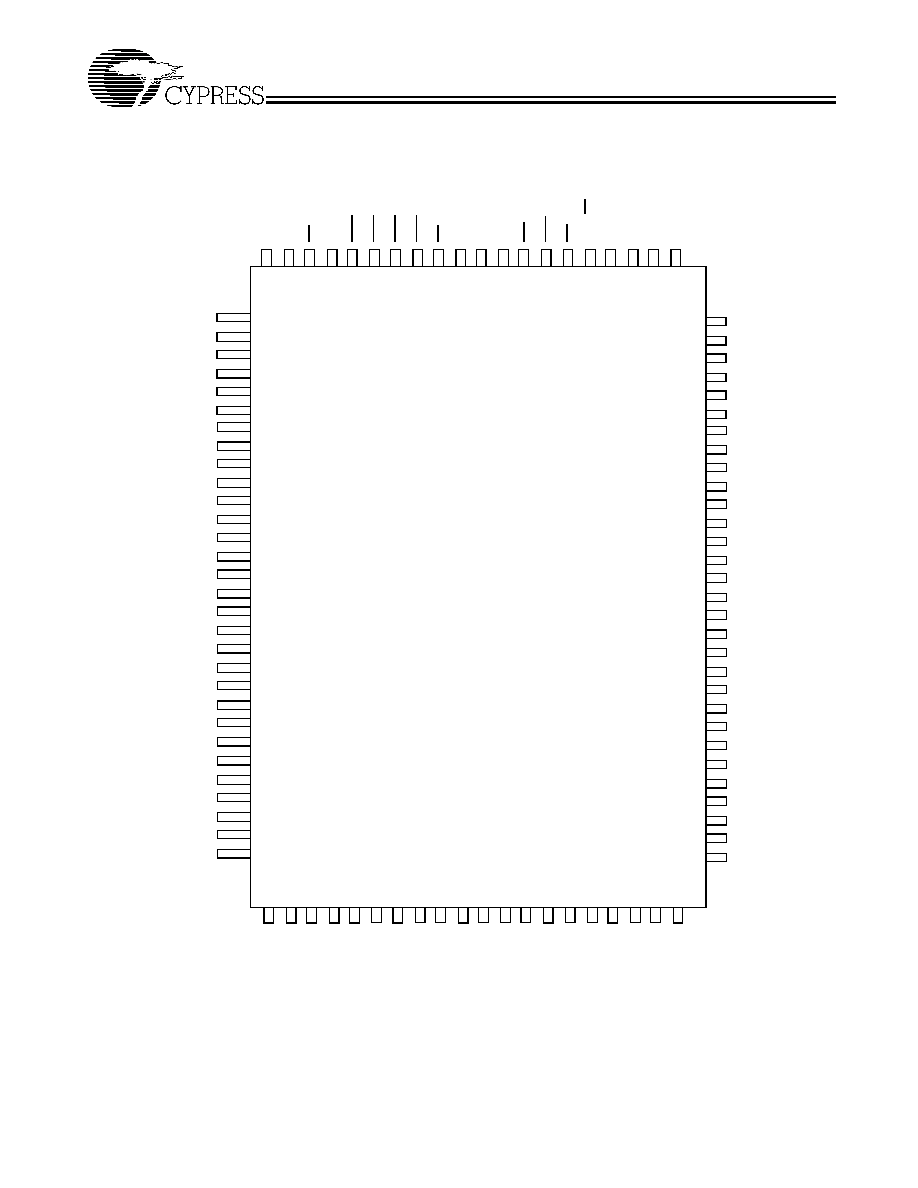
Pin Configuration
A
5
A
4
A
3
A
2
A
1
A
0
DNU
DNU
V
SS
V
DD
DNU
A
10
A
11
A
12
A
13
A
14
A
16
DP
1
DQ
15
DQ
14
V
DDQ
V
SS
DQ
13
DQ
12
DQ
11
DQ
10
V
SS
V
DDQ
DQ
9
DQ
8
V
SS
V
SS
V
DD
DQ
7
DQ
6
V
DDQ
V
SS
DQ
5
DQ
4
DQ
3
DQ
2
V
SS
V
DDQ
DQ
1
DQ
0
DP
0
DP
2
DQ
16
DQ
17
V
DDQ
V
SS
DQ
18
DQ
19
DQ
20
DQ
21
V
SS
V
DDQ
DQ
22
DQ
23
V
SS
V
DD
V
DD
V
SS
DQ
24
DQ
25
V
DDQ
V
SS
DQ
26
DQ
27
DQ
28
DQ
29
V
SS
V
DDQ
DQ
30
DQ
31
DP
3
A6
A7
CE
1
CE
2
BW
S
3
BW
S
2
BW
S
1
BW
S
0
CE
3
V
DD
V
SS
CLK
WE
CE
N
OE
A
8
A
9
1
2
3
4
5
6
7
8
9
10
11
12
13
14
15
16
17
18
19
20
21
22
23
24
25
26
27
28
29
30
31
32
33
34
35
36
37
38
39
40
41
42
43
44
45
46
47
48
49
50
80
79
78
77
76
75
74
73
72
71
70
69
68
67
66
65
64
63
62
61
60
59
58
57
56
55
54
53
52
51
100
99
98
97
96
95
94
93
92
91
90
89
88
87
86
85
84
83
82
81
A
15
AD
V/
LD
V
SS
MO
D
E
DNU
NC
NC
100-Pin TQFP
CY7C1351B
CY7C1351B
PRELIMINARY
Document #: 38-05208 Rev. *A
Page 3 of 16
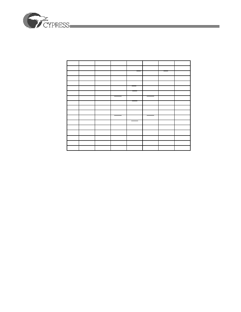
Pin Configuration
2
3
4
5
6
7
1
A
B
C
D
E
F
G
H
J
K
L
M
N
P
R
T
U
DQ
a
V
DDQ
NC
NC
DQ
c
DQ
d
DQ
c
DQ
d
A
A
A
A
16M
V
DDQ
CE
2
A
V
DDQ
V
DDQ
V
DDQ
V
DDQ
NC
NC
A
DQ
c
DQ
c
DQ
d
DQ
d
TMS
V
DD
A
64M
DP
d
A
A
ADV/LD
A
CE
3
NC
V
DD
A
A
NC
V
SS
V
SS
NC
DP
b
DQ
b
DQ
b
DQ
a
DQ
b
DQ
b
DQ
a
DQ
a
DNU
TDI
TDO
V
DDQ
TCK
V
SS
V
SS
V
SS
V
SS(1)
V
SS
V
SS
V
SS
V
SS
MODE
CE
1
V
SS
OE
V
SS
V
DDQ
BWS
c
8M
V
SS
WE
V
DDQ
V
DD
V
SS(1)
V
DD
V
SS
CLK
NC
BWS
a
CEN
V
SS
V
DDQ
V
SS
NC
NC
A
A
A1
A0
V
SS
V
DD
CY7C1351B (128K x 36) - 7 x 17 BGA
DP
c
DQ
b
A
32M
DQ
c
DQ
b
DQ
c
DQ
c
DQ
c
DQ
b
DQ
b
DQ
a
DQ
a
DQ
a
DQ
a
DP
a
DQ
d
DQ
d
DQ
d
DQ
d
BWS
d
119-Ball Bump BGA
BWS
b
V
SS
CY7C1351B
PRELIMINARY
Document #: 38-05208 Rev. *A
Page 4 of 16
Pin Definitions
Name
I/O
Description
A
[16:0]
Input-
Synchronous
Address Inputs used to select one of the 133,072 address locations. Sampled at the rising
edge of the CLK.
BWS
[3:0]
Input-
Synchronous
Byte Write Select Inputs, active LOW. Qualified with WE to conduct writes to the SRAM.
Sampled on the rising edge of CLK. BWS
0
controls DQ
[7:0]
and DP
0
, BWS
1
controls DQ
[15:8]
and DP
1
, BWS
2
controls DQ
[23:16]
and DP
2
, BWS
3
controls DQ
[31:24]
and DP
3
.
WE
Input-
Synchronous
Write Enable Input, active LOW. Sampled on the rising edge of CLK if CEN is active LOW.
This signal must be asserted LOW to initiate a write sequence.
ADV/LD
Input-
Synchronous
Advance/Load input used to advance the on-chip address counter or load a new ad-
dress. When HIGH (and CEN is asserted LOW) the internal burst counter is advanced. When
LOW, a new address can be loaded into the device for an access. After being deselected,
ADV/LD should be driven LOW in order to load a new address.
CLK
Input-Clock
Clock Input. Used to capture all synchronous inputs to the device. CLK is qualified with CEN.
CLK is only recognized if CEN is active LOW.
CE
1
Input-
Synchronous
Chip Enable 1 Input, active LOW. Sampled on the rising edge of CLK. Used in conjunction
with CE
2
and CE
3
to select/deselect the device.
CE
2
Input-
Synchronous
Chip Enable 2 Input, active HIGH. Sampled on the rising edge of CLK. Used in conjunction
with CE
1
and CE
3
to select/deselect the device.
CE
3
Input-
Synchronous
Chip Enable 3 Input, active LOW. Sampled on the rising edge of CLK. Used in conjunction
with CE
1
and
CE
2
to select/deselect the device.
OE
Input-
Asynchronous
Output Enable, active LOW. Combined with the synchronous logic block inside the device to
control the direction of the I/O pins. When LOW, the I/O pins are allowed to behave as outputs.
When deasserted HIGH, I/O pins are three-stated, and act as input data pins. OE is masked
during the data portion of a write sequence, during the first clock when emerging from a
deselected state and when the device has been deselected.
CEN
Input-
Synchronous
Clock Enable Input, active LOW. When asserted LOW the clock signal is recognized by the
SRAM. When deasserted HIGH the clock signal is masked. Since deasserting CEN does not
deselect the device, CEN can be used to extend the previous cycle when required.
DQ
[31:0]
I/O-
Synchronous
Bidirectional Data I/O Lines. As inputs, they feed into an on-chip data register that is triggered
by the rising edge of CLK. As outputs, they deliver the data contained in the memory location
specified by A
[16:0]
during the previous clock rise of the read cycle. The direction of the pins is
controlled by OE and the internal control logic. When OE is asserted LOW, the pins can behave
as outputs. When HIGH, DQ
[31:0]
are placed in a three-state condition. The outputs are auto-
matically three-stated during the data portion of a write sequence, during the first clock when
emerging from a deselected state, and when the device is deselected, regardless of the state
of OE.
DP
[3:0]
I/O-
Synchronous
Bidirectional Data Parity I/O Lines. Functionally, these signals are identical to DQ
[31:0]
. Dur-
ing write sequences, DP
0
is controlled by BWS
0
, DP
1
is controlled by BWS
1
, DP
2
is controlled
by BWS
2
, and DP
3
is controlled by BWS
3
.
MODE
Input
Strap pin
Mode Input. Selects the burst order of the device. Tied HIGH selects the interleaved burst
order. Pulled LOW selects the linear burst order. MODE should not change states during
operation. When left floating MODE will default HIGH, to an interleaved burst order.
V
DD
Power Supply
Power supply inputs to the core of the device. Should be connected to 3.3V power supply.
V
DDQ
I/O Power
Supply
Power supply for the I/O circuitry. Should be connected to a 3.3V power supply.
V
SS
Ground
Ground for the device. Should be connected to ground of the system.
NC
-
No Connects. Reserved for address inputs for depth expansion. Pins 83 and 84 will be used
for 256K and 512K depths respectively.
DNU
-
Do Not Use pins. These pins should be left floating or tied to V
SS
.

CY7C1351B
PRELIMINARY
Document #: 38-05208 Rev. *A
Page 5 of 16
Introduction
Functional Overview
The CY7C1351B is a Synchronous Flow-Through Burst
SRAM designed specifically to eliminate wait states during
Write-Read transitions. All synchronous inputs pass through
input registers controlled by the rising edge of the clock. The
clock signal is qualified with the Clock Enable input signal
(CEN). If CEN is HIGH, the clock signal is not recognized and
all internal states are maintained. All synchronous operations
are qualified with CEN. Maximum access delay from the clock
rise (t
CDV
) is 7.5 ns (117-MHz device).
Accesses can be initiated by asserting all three Chip Enables
(CE
1
, CE
2
, CE
3
) active at the rising edge of the clock. If Clock
Enable (CEN) is active LOW and ADV/LD is asserted LOW,
the address presented to the device will be latched. The ac-
cess can either be a Read or Write operation, depending on
the status of the Write Enable (WE). BWS
[3:0]
can be used to
conduct byte write operations.
Write operations are qualified by the Write Enable (WE). All
writes are simplified with on-chip synchronous self-timed write
circuitry.
Three synchronous Chip Enables (CE
1
, CE
2
, CE
3
) and an
asynchronous Output Enable (OE) simplify depth expansion.
All operations (Reads, Writes, and Deselects) are pipelined.
ADV/LD should be driven LOW once the device has been de-
selected in order to load a new address for the next operation.
Single Read Accesses
A read access is initiated when the following conditions are
satisfied at clock rise: (1) CEN is asserted LOW, (2) CE
1
, CE
2
and CE
3
are ALL asserted active, (3) the Write Enable input
signal WE is deasserted HIGH, and 4) ADV/LD is asserted
LOW. The address presented to the address inputs (A
0
A
16
)
is latched into the Address Register and presented to the
memory core and control logic. The control logic determines
that a read access is in progress and allows the requested
data to propagate to the output buffers. The data is available
within 7.5 ns (117-MHz device) provided OE is active LOW.
After the first clock of the read access the output buffers are
controlled by OE and the internal control logic. OE must be
driven LOW in order for the device to drive out the requested
data. On the subsequent clock, another operation
(Read/Write/Deselect) can be initiated. When the SRAM is de-
selected at clock rise by one of the chip enable signals, its
output will three-stated immediately.
Burst Read Accesses
The CY7C1351B has an on-chip burst counter that allows the
user the ability to supply a single address and conduct up to
four Reads without reasserting the address inputs. ADV/LD
must be driven LOW in order to load a new address into the
SRAM, as described in the Single Read Access section above.
The sequence of the burst counter is determined by the MODE
input signal. A LOW input on MODE selects a linear burst
mode, a HIGH selects an interleaved burst sequence. Both
burst counters use A0 and A1 in the burst sequence, and will
wrap around when incremented sufficiently. A HIGH input on
ADV/LD will increment the internal burst counter regardless of
the state of chip enables inputs or WE. WE is latched at the
beginning of a burst cycle. Therefore, the type of access (Read
or Write) is maintained throughout the burst sequence.
Single Write Accesses
Write access are initiated when the following conditions are
satisfied at clock rise: (1) CEN is asserted LOW, (2) CE
1
, CE
2
,
and CE
3
are ALL asserted active, and (3) the write signal WE
is asserted LOW. The address presented to A
0
A
16
is loaded
into the Address Register. The write signals are latched into
the Control Logic block. The data lines are automatically
three-stated regardless of the state of the OE input signal. This
allows the external logic to present the data on DQ
[31:0]
and
DP
[3:0]
.
On the next clock rise the data presented to DQ
[31:0]
and
DP
[3:0]
(or a subset for byte write operations, see Write Cycle
Description table for details) inputs is latched into the device
and the write is complete. Additional accesses
(Read/Write/Deselect) can be initiated on this cycle.
The data written during the Write operation is controlled by
BWS
[3:0]
signals. The CY7C1351B provides byte write capa-
bility that is described in the Write Cycle Description table.
Asserting the Write Enable input (WE) with the selected Byte
Write Select (BWS
[3:0]
) input will selectively write to only the
desired bytes. Bytes not selected during a byte write operation
will remain unaltered. A synchronous self-timed write mecha-
nism has been provided to simplify the write operations. Byte
write capability has been included in order to greatly simplify
Read/Modify/Write sequences, which can be reduced to sim-
ple byte write operations.
Because the CY7C1351B is a common I/O device, Data
should not be driven into the device while the outputs are ac-
tive. The Output Enable (OE) can be deasserted HIGH before
presenting data to the DQ
[31:0]
and DP
[3:0]
inputs. Doing so will
three-state the output drivers. As a safety precaution, DQ
[31:0]
and DP
[3:0]
.are automatically three-stated during the data por-
tion of a write cycle, regardless of the state of OE.
Burst Write Accesses
The CY7C1351B has an on-chip burst counter that allows the
user the ability to supply a single address and conduct up to
four Write operations without reasserting the address inputs.
ADV/LD must be driven LOW in order to load the initial ad-
dress, as described in the Single Write Access section above.
When ADV/LD is driven HIGH on the subsequent clock rise,
the chip enables (CE
1
, CE
2
, and CE
3
) and WE inputs are ig-
nored and the burst counter is incremented. The correct
BWS
[3:0]
inputs must be driven in each cycle of the burst write
in order to write the correct bytes of data.