 | –≠–Ľ–Ķ–ļ—ā—Ä–ĺ–Ĺ–Ĺ—č–Ļ –ļ–ĺ–ľ–Ņ–ĺ–Ĺ–Ķ–Ĺ—ā: W40S11 | –°–ļ–į—á–į—ā—Ć:  PDF PDF  ZIP ZIP |
SDRAM Buffer - 2 DIMM (Mobile)
W40S11-02
Cypress Semiconductor Corporation
∑
3901 North First Street
∑
San Jose
∑
CA 95134
∑
408-943-2600
September 29, 1999, rev. **
Features
∑ Ten skew-controlled CMOS outputs (SDRAM0:9)
∑ Supports two SDRAM DIMMs
∑ Ideal for high-performance systems designed around
Intelģ's latest Mobile chip set
∑ I
2
C Serial configuration interface
∑ Skew between any two outputs is less than 250 ps
∑ 1 to 5 ns propagation delay
∑ DC to 133-MHz operation
∑ Single 3.3V supply voltage
∑ Low power CMOS design packaged in a 28-pin, 209-mil
SSOP (Shrink Small Outline Package)
Overview
The Cypress W40S11-02 is a low-voltage, ten-output clock
buffer. Output buffer impedance is approximately 15
, which
is ideal for driving SDRAM DIMMs.
Key Specifications
Supply Voltages:........................................... V
DD
= 3.3VĪ5%
Operating Temperature:.................................... 0įC to +70įC
Input Threshold: .................................................. 1.5V typical
Maximum Input Voltage: .......................................V
DD
+ 0.5V
Input Frequency:............................................... 0 to 133 MHz
BUF_IN to SDRAM0:9 Propagation Delay: ........1.0 to 5.0 ns
Output Edge Rate:................................................. >1.5 V/ns
Output Skew: ............................................................ Ī250 ps
Output Duty Cycle: .................................. 45/55% worst case
Output Impedance: ........................................15 ohms typical
Output Type: ................................................ CMOS rail-to-rail
Intel is a registered trademark of Intel Corporation.
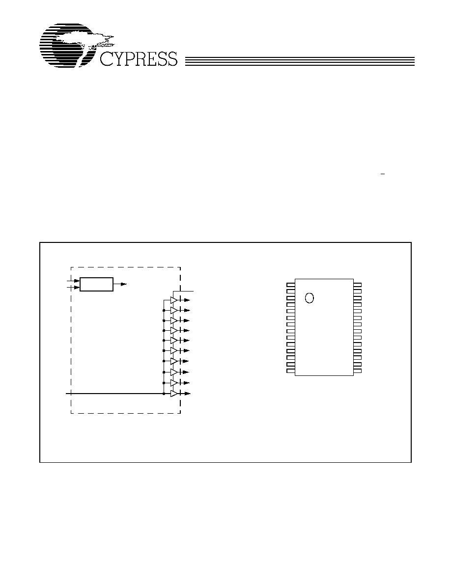
Pin Configuration
Block Diagram
Note:
1.
Internal pull-up resistor of 250K on SDATA, SCLOCK, and OE
inputs (should not be relied upon for pulling up to V
DD
).
[1]
[1]
SDRAM1
SDRAM2
SDRAM3
SDRAM4
SDRAM5
SDRAM6
SDRAM7
SDRAM8
SDRAM9
SDRAM0
Serial Port
SCLOCK
SDATA
Device Control
BUF_IN
OE
VDD
SDRAM0
SDRAM1
GND
VDD
SDRAM2
SDRAM3
GND
BUF_IN
VDD
SDRAM8
GND
VDD
SDATA
VDD
SDRAM7
SDRAM6
GND
VDD
SDRAM5
SDRAM4
GND
OE
VDD
SDRAM9
GND
GND
SCLOCK
28
27
26
25
24
23
22
21
20
19
18
17
16
15
1
2
3
4
5
6
7
8
9
10
11
12
13
14
[1]
W40S11-02
2
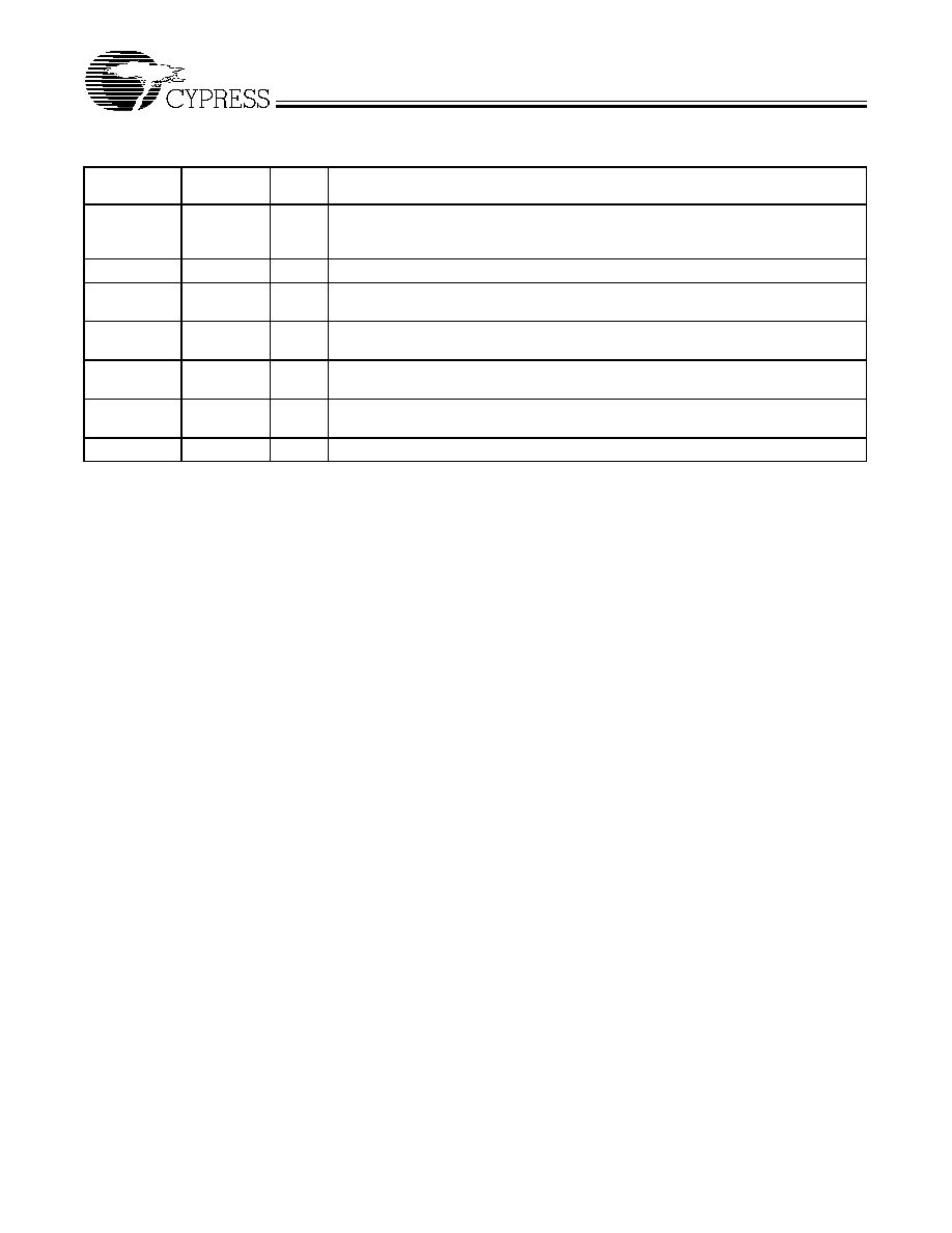
Pin Definitions
Pin Name
Pin
No.
Pin
Type
Pin Description
SDRAM0:9
2, 3, 6, 7,
22, 23, 26,
27, 11, 18
O
SDRAM Outputs: Provides buffered copy of BUF_IN. The propagation delay from a
rising input edge to a rising output edge is 1 to 5 ns. All outputs are skew controlled
to within Ī 250 ps of each other.
BUF_IN
9
I
Clock Input: This clock input has an input threshold voltage of 1.5V (typ).
SDATA
14
I/O
I
2
C Data Input: Data should be presented to this input as described in the I
2
C section
of this data sheet. Internal 250-k
pull-up resistor.
SCLOCK
15
I
I
2
C Clock Input: The I
2
C Data clock should be presented to this input as described
in the I
2
C section of this data sheet. Internal 250-k
pull-up resistor.
VDD
1, 5, 10, 13,
19, 24, 28
P
Power Connection: Power supply for core logic and output buffers. Connected to
3.3V supply.
GND
4, 8, 12, 16,
17, 21, 25
G
Ground Connection: Connect all ground pins to the common system ground plane.
OE
20
I
Output Enable: Internal 250-k
pull-up resistor. Three-states outputs when LOW.
W40S11-02
3
Functional Description
Output Control Pins
Outputs three-stated when OE = 0, and toggle when OE = 1.
Outputs are in phase with BUF_IN but are phase delayed by 1
to 5 ns. Outputs can also be controlled via the I
2
C interface.
Output Drivers
The W40S11-02 output buffers are CMOS type which deliver
a rail-to-rail (GND to V
DD
) output voltage swing into a nominal
capacitive load. Thus, output signaling is both TTL and CMOS
level compatible. Nominal output buffer impedance is 15 ohms.
Operation
Data is written to the W40S11-02 in ten bytes of eight bits
each. Bytes are written in the order shown in Table 1.
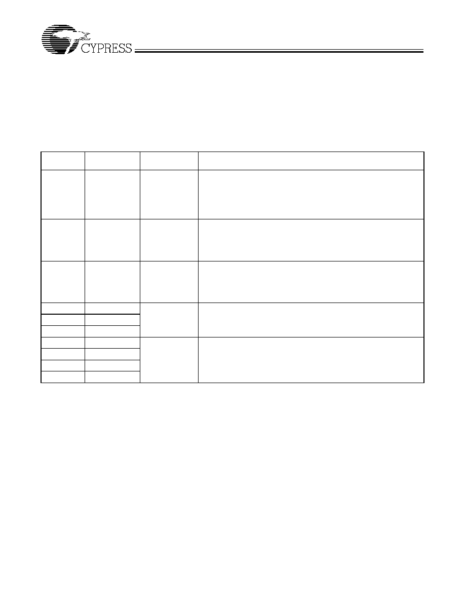
Table 1. Byte Writing Sequence
Byte
Sequence
Byte Name
Bit Sequence
Byte Description
1
Slave Address
11010010
Commands the W40S11-02 to accept the bits in Data Bytes 0≠6 for in-
ternal register configuration. Since other devices may exist on the same
common serial data bus, it is necessary to have a specific slave address
for each potential receiver. The slave receiver address for the W40S11-02
is 11010010. Register setting will not be made if the Slave Address is not
correct (or is for an alternate slave receiver).
2
Command
Code
Don't Care
Unused by the W40S11-02, therefore bit values are ignored (don't care).
This byte must be included in the data write sequence to maintain proper
byte allocation. The Command Code Byte is part of the standard serial
communication protocol and may be used when writing to another ad-
dressed slave receiver on the serial data bus.
3
Byte Count
Don't Care
Unused by the W40S11-02, therefore bit values are ignored (don't care).
This byte must be included in the data write sequence to maintain proper
byte allocation. The Byte Count Byte is part of the standard serial com-
munication protocol and may be used when writing to another addressed
slave receiver on the serial data bus.
4
Data Byte 0
Refer to Table 2
The data bits in these bytes set internal W40S11-23 registers that control
device operation. The data bits are only accepted when the Address Byte
bit sequence is 11010010, as noted above. For description of bit control
functions, refer to Table 2, Data Byte Serial Configuration Map.
5
Data Byte 1
6
Data Byte 2
7
Data Byte 3
Don't Care
Refer to Cypress clock drivers.
8
Data Byte 4
9
Data Byte 5
10
Data Byte 6
W40S11-02
4
Writing Data Bytes
Each bit in the data bytes control a particular device function.
Bits are written MSB (most significant bit) first, which is bit 7.
Table 2 gives the bit formats for registers located in Data Bytes
0≠6.
Note:
2.
At power-up all SDRAM outputs are enabled and active. It is recommended to program Bits 4≠7 of Byte0 and Bits 0≠3 of Byte1 to a "0" to save power and reduce
noise.
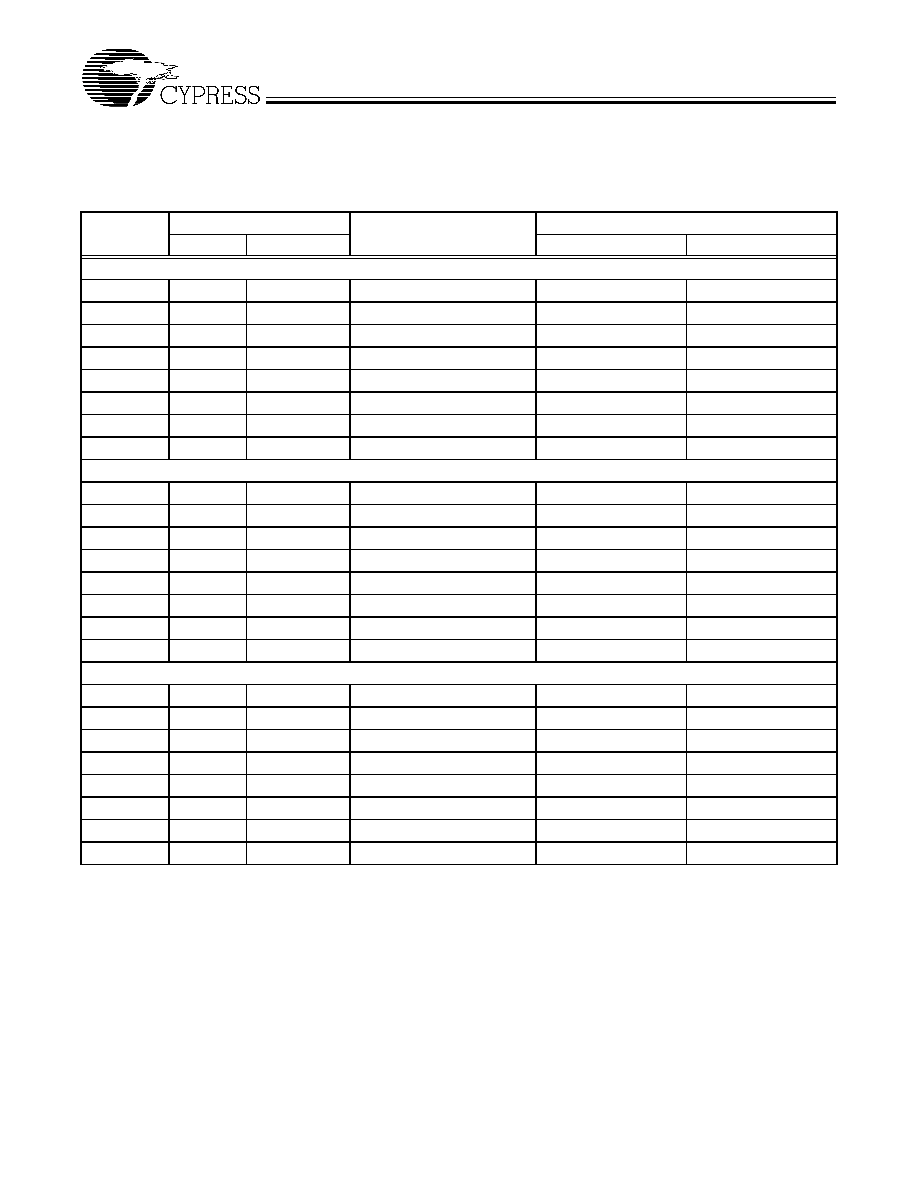
Table 2. Data Bytes 0≠2 Serial Configuration Map
[2]
Bit(s)
Affected Pin
Control Function
Bit Control
Pin No.
Pin Name
0
1
Data Byte 0 SDRAM Active/Inactive Register (1=Enable, 0=Disable)
7
N/A
Reserved
(Reserved)
--
--
6
N/A
Reserved
(Reserved)
--
--
5
N/A
Reserved
(Reserved)
--
--
4
N/A
Reserved
(Reserved)
--
--
3
7
SDRAM3
Clock Output Disable
Low
Active
2
6
SDRAM2
Clock Output Disable
Low
Active
1
3
SDRAM1
Clock Output Disable
Low
Active
0
2
SDRAM0
Clock Output Disable
Low
Active
Data Byte 1 SDRAM Active/Inactive Register (1=Enable, 0=Disable)
7
27
SDRAM7
Clock Output Disable
Low
Active
6
26
SDRAM6
Clock Output Disable
Low
Active
5
23
SDRAM5
Clock Output Disable
Low
Active
4
22
SDRAM4
Clock Output Disable
Low
Active
3
N/A
Reserved
(Reserved)
--
--
2
N/A
Reserved
(Reserved)
--
--
1
N/A
Reserved
(Reserved)
--
--
0
N/A
Reserved
(Reserved)
--
--
Data Byte 2 SDRAM Active/Inactive Register (1=Enable, 0=Disable)
7
18
SDRAM9
Clock Output Disable
Low
Active
6
11
SDRAM8
Clock Output Disable
Low
Active
5
N/A
Reserved
(Reserved)
--
--
4
N/A
Reserved
(Reserved)
--
--
3
N/A
Reserved
(Reserved)
--
--
2
N/A
Reserved
(Reserved)
--
--
1
N/A
Reserved
(Reserved)
--
--
0
N/A
Reserved
(Reserved)
--
--

W40S11-02
5
How To Use the Serial Data Interface
Electrical Requirements
Figure 1 illustrates electrical characteristics for the serial inter-
face bus used with the W40S11-02. Devices send data over
the bus with an open drain logic output that can (a) pull the bus
line LOW, or (b) let the bus default to logic 1. The pull-up resis-
tor on the bus (both clock and data lines) establish a default
logic 1. All bus devices generally have logic inputs to receive
data.
Although the W40S11-02 is a receive-only device (no data
write-back capability), it does transmit an "acknowledge" data
pulse after each byte is received. Thus, the SDATA line can
both transmit and receive data.
The pull-up resistor should be sized to meet the rise and fall
times specified in AC parameters, taking into consideration to-
tal bus line capacitance.
DATA IN
DATA OUT
N
CLOCK IN
C L O C K O U T
CHIP SET
(SERIAL BUS MASTER TRANSMITTER)
S D C L K
SDATA
SERIAL BUS CLOCK LINE
SERIAL BUS DATA LINE
N
DATA IN
DATA OUT
CLOCK IN
C L O C K D E V I C E
(SERIAL BUS SLAVE RECEIVER)
S C L O C K
SDATA
N
~ 2k
~ 2k
V D D
V D D
Figure 1. Serial Interface Bus Electrical Characteristics