Äîêóìåíòàöèÿ è îïèñàíèÿ www.docs.chipfind.ru
PRELIMINARY
Spread Spectrum Motherboard Frequency Generator
W48S101-04
Cypress Semiconductor Corporation
·
3901 North First Street
·
San Jose
·
CA 95134
·
408-943-2600
October 27, 1999, rev. **
Features
· Maximized EMI suppression using Cypress's Spread
Spectrum technology
· I
2
CTM interface
· Four copies of CPU output
· Eight copies of PCI clock (synchronous w/CPU output)
· Two copies of 14.318-MHz IOAPIC output
· One copy of 48-MHz USB output
· Selectable 24-/48-MHz clock-through-resistor
strapping
· Three buffered copies of 14.318-MHz reference input
· Input is a 14.318-MHz XTAL or reference signal
· Selectable 100-MHz or 66-MHz CPU outputs
· Power management control input pins
· Test mode and output three-state through I
2
C interface
Key Specifications
Supply Voltages:....................................... V
DDQ3
= 3.3V±5%
V
DDQ2
= 2.5V±5%
CPU Cycle to Cycle Jitter: ........................................... 200 ps
CPU0:3 Output Skew: ................................................ 175 ps
PCI_F, PCI1:7 Output Skew: .......................................500 ps
CPU to PCI Output Skew: ............ 1.5 to 4.0 ns (CPU Leads)
Logic inputs and REF0/SEL48# have 250K pull-up resistors
except SEL100/66#.
I
2
C is a trademark of Philips Corporation.
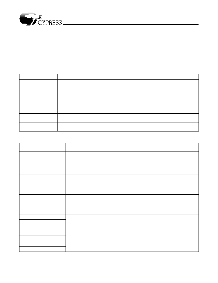
Table 1. Pin Selectable Frequency
SEL
100/66#
CPU (MHz)
PCI
(MHz)
SPREAD#=0
0
66.8
33.4
±0.5% Center
1
100
33.3
±0.5% Center
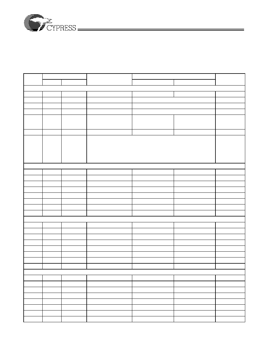
Pin Configuration
Block Diagram
VDDREF
REF0/SEL48#
VDDAPIC
APIC0
CPU0
CPU1
CPU2
CPU3
PCI_F
XTAL
PLL Ref Freq
PLL 1
100/66#_SEL
X2
X1
REF1
VDDPCI0
Stop
Clock
Control
Stop
Clock
Control
PCI1
PWR_DWN#
Power
Down
Control
PCI2
PCI3
PCI4
PCI5
48MHz
24/48MHz
PLL2
÷2/÷3
OSC
REF2
VDDCPU0
PCI_STOP#
CPU_STOP#
PCI6
PCI7
GNDPCI1
GND48MHz
VDD48MHz
GNDREF
APIC1
GNDAPIC
GNDCORE0/1
VDDCORE0/1
VDDPCI1
GNDPCI0
GNDCPU1
GNDCPU0
VDDCPU1
SPREAD#
I
2
C
SDATA
Logic
SCLK
REF0/SEL48#
REF1
GNDREF
X1
X2
GNDPCI0
PCICLK_F
PCI1
VDDPCI0
PCI2
PCI3
GNDPCI1
PCI4
PCI5
VDDPCI1
PCI6
PCI7
GNDPCI2
VDDCORE0
GNDCORE0
VDD48MHz
48MHz
24/48MHz
GND48MHz
VDDREF
REF2
VDDAPIC
APIC0
APIC1
GNDAPIC
NC
VDDCPU0
CPU0
CPU1
GNDCPU0
VDDCPU1
CPUCLK2
CPUCLK3
GNDCPU1
VDDCORE1
GNDCORE1
PCI_STOP#
CPU_STOP#
PWR_DWN#
SPREAD#
SDATA
SCLK
SEL100/66#
48
47
46
45
44
43
42
41
40
39
38
37
36
35
34
33
32
31
30
29
28
27
26
25
1
2
3
4
5
6
7
8
9
10
11
12
13
14
15
16
17
18
19
20
21
22
23
24
Note:
1.
Internal pull-up resistors should not be relied upon for
setting I/O pins HIGH.
[1]
W48S101-04
PRELIMINARY
2
Pin Definitions
Pin Name
Pin No.
Pin Type
Pin Description
CPU0:3
40, 39, 36,
35
O
CPU Clock Outputs 0 through 3: These four CPU clock outputs are controlled by
the CPU_STOP# control pin. Output voltage swing is controlled by voltage applied
to VDDQ2.
PCI1:7
8, 10, 11,
13, 14, 16,
17
O
PCI Bus Clock Outputs 1 through 7: These seven PCI clock outputs are controlled
by the PCI_STOP# control pin. Output voltage swing is controlled by voltage applied
to VDDQ3.
PCI_F
7
O
Fixed PCI Clock Output: Unlike PCI1:7 outputs, this output is not controlled by the
PCI_STOP# control pin. Output voltage swing is controlled by voltage applied to
VDDQ3.
CPU_STOP#
30
I
CPU_STOP# Input: When brought LOW, clock outputs CPU0:3 are stopped LOW
after completing a full clock cycle (23 CPU clock latency). When brought HIGH,
clock outputs CPU0:3 start beginning with a full clock cycle (23 CPU clock latency).
PCI_STOP#
31
I
PCI_STOP# Input: The PCI_STOP# input enables the PCI 1:7 outputs when HIGH
and causes them to remain at logic 0 when LOW. The PCI_STOP signal is latched
on the rising edge of PCI_F. Its effect takes place on the next PCI_F clock cycle.
SPREAD#
28
I
SPREAD# Input: When brought LOW this pin activates Spread Spectrum clocking.
APIC0:1
45, 44
O
I/O APIC Clock Outputs: Provides 14.318-MHz fixed frequency. The output voltage
swing is controlled by VDDQ2.
48MHz
22
O
48-MHz Output: Fixed clock outputs at 48 MHz. Output voltage swing is controlled
by voltage applied to VDDQ3.
24/48MHz
23
O
24-MHz or 48-MHz Output: 24-MHz output when pin 1 is strapped through 10-k
resistor to VDDQ3. 48-MHz output when pin 1 is strapped through 10-k
resistor to
GND.
REF0/SEL48#
1
I/O
I/O Dual Function REF0 and SEL48# pin: During power on, SEL48# input will be
latched, which will set pin 23 to output 24 MHz or 48 MHz. It then reverts to REF0
fixed output.
REF1:2
2, 47
O
Fixed 14.318-MHz Outputs 1 through 2: Used for various system applications.
Output voltage swing is controlled by voltage applied to VDDQ3.
SEL100/66#
25
I
Frequency Selection Input: Selects power-up default CPU clock frequency as
shown in Table 1 on page 1.
SCLK
26
I
Clock pin for I
2
C circuitry.
SDATA
27
I/O
Data pin for I
2
C circuitry.
X1
4
I
Crystal Connection or External Reference Frequency Input: This pin has dual
functions. It can be used as an external 14.318-MHz crystal connection or as an
external reference frequency input.
X2
5
I
Crystal Connection: An input connection for an external 14.318-MHz crystal. If
using an external reference, this pin must be left unconnected.
PWR_DWN#
29
I
Power Down Control: When this input is LOW, device goes into a low-power stand-
by condition. All outputs are actively held LOW while in power-down. CPU and PCI
clock outputs are stopped LOW after completing a full clock cycle (23 CPU clock
cycle latency). When brought HIGH, CPU, SDRAM and PCI outputs start with a full
clock cycle at full operating frequency (3 ms maximum latency).
VDDQ3
9, 15, 19,
21, 33, 48
P
Power Connection: Connect to 3.3V supply.
VDDQ2
46, 41, 37
P
Power Connection: Power supply for APIC0:1 and CPU0:3 output buffers. Connect
to 2.5V.
GND
3, 6, 12, 18,
20, 24, 32,
34, 38, 43
G
Ground Connections: Connect all ground pins to the common system ground
plane.
W48S101-04
PRELIMINARY
3
Overview
The W48S101-04, a motherboard clock synthesizer, can pro-
vide either a 2.5V or 3.3V CPU clock swing, making it suitable
for a variety of CPU options. A fixed 48-MHz clock is provided
for other system functions. The W48S101-04 supports spread
spectrum clocking for reduced EMI.
Functional Description
I/O Pin Operation
Pin 1 is a dual-purpose l/O pin. Upon power-up this pin acts as
a logic input, allowing the determination of assigned device
functions. A short time after power-up, the logic state of the pin
is latched and the pin becomes a clock output. This feature
reduces device pin count by combining clock outputs with input
select pins.
An external 10-k
"strapping" resistor is connected between
the l/O pin and ground or V
DD
. Connection to ground sets a
latch to "0," connection to V
DD
sets a latch to "1." Figure 1 and
Figure 2 show two suggested methods for strapping resistor
connections.
Upon W48S101-04 power-up, the first 2 ms of operation is
used for input logic selection. During this period, the Refer-
ence clock output buffer is three-stated, allowing the output
strapping resistor on the l/O pin to pull the pin and its associ-
ated capacitive clock load to either a logic HIGH or LOW state.
At the end of the 2-ms period, the established logic "0" or "1"
condition of the l/O pin is then latched. Next the output buffer
is enabled, which converts the l/O pin into an operating clock
output. The 2-ms timer is started when V
DD
reaches 2.0V. The
input bit can only be reset by turning V
DD
off and then back on
again.
It should be noted that the strapping resistor has no significant
effect on clock output signal integrity. The drive impedance of
clock output is 40
(nominal) which is minimally affected by
the 10-k
strap to ground or V
DD
. As with the series termina-
tion resistor, the output strapping resistor should be placed as
close to the l/O pin as possible in order to keep the intercon-
necting trace short. The trace from the resistor to ground or
V
DD
should be kept less than two inches in length to prevent
system noise coupling during input logic sampling.
When the clock output is enabled following the 2-ms input pe-
riod, a 14.318-MHz output frequency is delivered on the pin,
assuming that V
DD
has stabilized. If V
DD
has not yet reached
full value, output frequency initially may be below target but will
increase to target once V
DD
voltage has stabilized. In either
case, a short output clock cycle may be produced from the
CPU clock outputs when the outputs are enabled.
Power-on
Reset
Timer
Output Three-state
Data
Latch
Hold
Q
D
W48S101-04
V
DD
Clock Load
10 k
Output
Buffer
(Load Option 1)
10 k
(Load Option 0)
Output
Low
Output Strapping Resistor
Series Termination Resistor
Figure 1. Input Logic Selection Through Resistor Load Option
Power-on
Reset
Timer
Output Three-state
Data
Latch
Hold
Q
D
W48S101-04
V
DD
Clock Load
R
10 k
Output
Buffer
Output
Low
Output Strapping Resistor
Series Termination Resistor
Jumper Options
Resistor Value R
Figure 2. Input Logic Selection Through Jumper Option
W48S101-04
PRELIMINARY
4
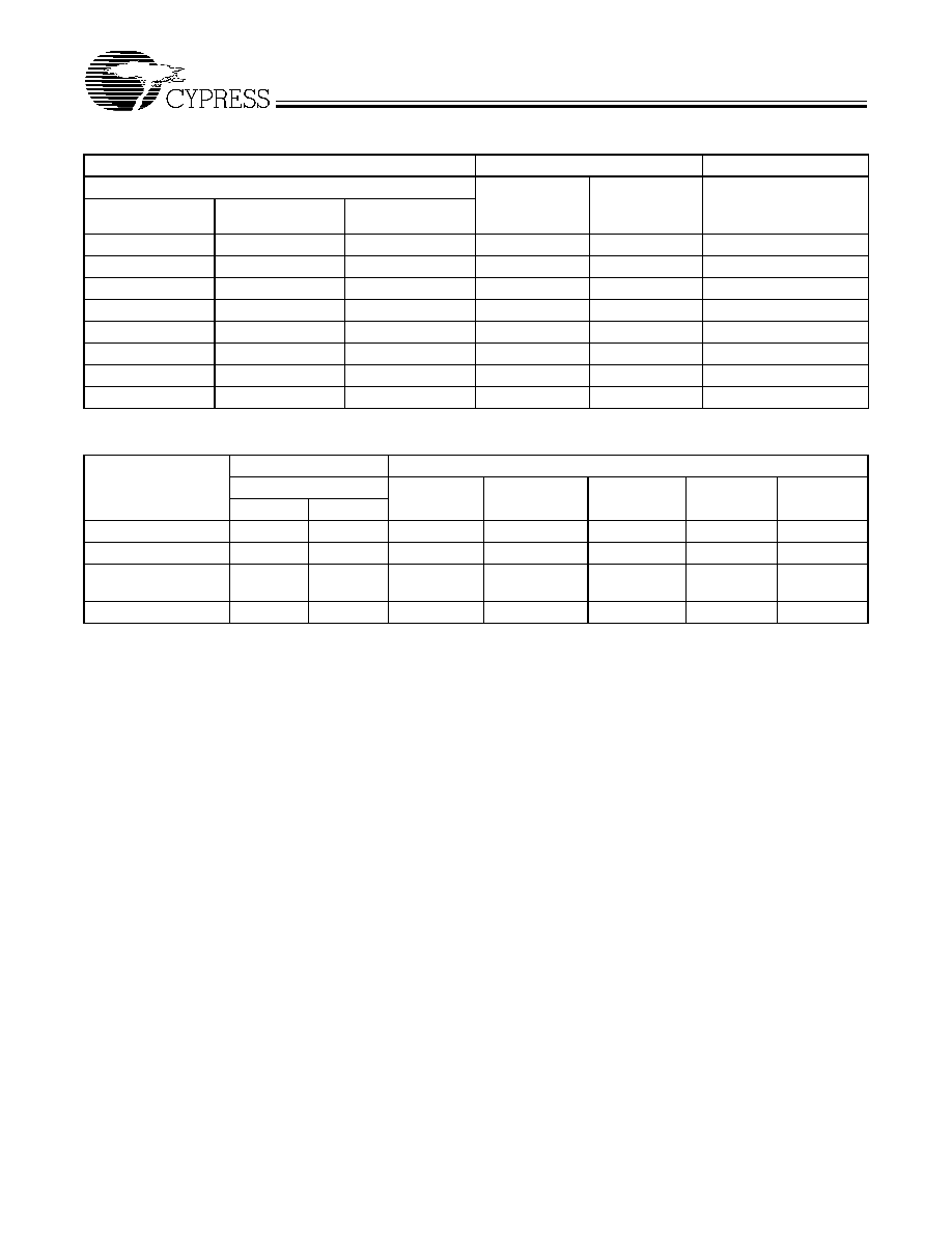
Spread Spectrum Clock Generation
The benefits of using Spread Spectrum Clock Generation are
depicted in Figure 3. An EMI emission profile of a clock har-
monic is shown.
Contrast the typical clock EMI with the Cypress Spread Spec-
trum Clock Generation. Notice the spike in the typical clock.
This spike can make systems fail quasi-peak EMI testing. The
FCC and other regulatory agencies test for peak emissions.
With the Cypress clock, the peak energy is much lower (at
least 8 dB) because the energy is spread out across a wider
bandwidth.
Figure 3. Typical Clock and SSCG Comparison
SS FT G
Ty p ic a l C lo ck
Freq ue n c y Sp an (M H z)
-SS %
+S S%
A
m
pl
i
t
ud
e
(
d
B
)
5dB/div
MAX (+0.5%)
MIN (0.5%)
10%
20%
30%
40%
50%
60%
70%
80%
90%
1
00%
10%
20%
30%
40%
50%
60%
70%
80%
90%
1
00%
FREQ
UENC
Y
Figure 4. Typical Modulation Profile
W48S101-04
PRELIMINARY
5
Serial Data Interface
The W48S101-04 features a two-pin, serial data interface that
can be used to configure internal register settings that control
particular device functions. Upon power-up, the W48S101-04
initializes with default register settings. Therefore, the use of
this serial data interface is optional. The serial interface is
write-only (to the clock chip) and is the dedicated function of
device pins SDATA and SCLOCK. In motherboard applica-
tions, SDATA and SCLOCK are typically driven by two logic
outputs of the chipset. Clock device register changes are nor-
mally made upon system initialization, if required. The inter-
face can also be used during system operation for power man-
agement functions. Table 2 summarizes the control functions
of the serial data interface.
Operation
Data is written to the W48S101-04 in ten bytes of eight bits
each. Bytes are written in the order shown in Table 3.
Table 2. Serial Data Interface Control Functions Summary
Control Function
Description
Common Application
Clock Output Disable
Any individual clock output(s) can be disabled. Dis-
abled outputs are actively held LOW.
Unused outputs are disabled to reduce EMI
and system power. Examples are clock out-
puts to unused PCI slots.
CPU Clock Frequency
Selection
Provides CPU/PCI frequency selections beyond the
100- and 66.6-MHz selections that are provided by
the SEL100/66# pin. Frequency is changed in a
smooth and controlled fashion.
For alternate microprocessors and power
management options. Smooth frequency tran-
sition allows CPU frequency change under
normal system operation.
Output Three-state
Puts all clock outputs into a high-impedance state.
Production PCB testing.
Test Mode
All clock outputs toggle in relation to X1 input, inter-
nal PLL is bypassed. Refer to Table 4.
Production PCB testing.
(Reserved)
Reserved function for future device revision or pro-
duction device testing.
No user application. Register bit must be writ-
ten as 0.
Table 3. Byte Writing Sequence
Byte
Sequence
Byte Name
Bit Sequence
Byte Description
1
Slave Address
11010010
Commands the W48S101-04 to accept the bits in Data Bytes 36 for
internal register configuration. Since other devices may exist on the same
common serial data bus, it is necessary to have a specific slave address
for each potential receiver. The slave receiver address for the
W48S101-04 is 11010010. Register setting will not be made if the Slave
Address is not correct (or is for an alternate slave receiver).
2
Command
Code
Don't Care
Unused by the W48S101-04, therefore bit values are ignored ("don't
care"). This byte must be included in the data write sequence to maintain
proper byte allocation. The Command Code Byte is part of the standard
serial communication protocol and may be used when writing to another
addressed slave receiver on the serial data bus.
3
Byte Count
Don't Care
Unused by the W48S101-04, therefore bit values are ignored ("don't
care"). This byte must be included in the data write sequence to maintain
proper byte allocation. The Byte Count Byte is part of the standard serial
communication protocol and may be used when writing to another ad-
dressed slave receiver on the serial data bus.
4
Data Byte 0
Don't Care
Refer to Cypress SDRAM drivers.
5
Data Byte 1
6
Data Byte 2
7
Data Byte 3
Refer to Table 4
The data bits in these bytes set internal W48S101-04 registers that con-
trol device operation. The data bits are only accepted when the Address
Byte bit sequence is 11010010, as noted above. For description of bit
control functions, refer to Table 4, Data Byte Serial Configuration Map.
8
Data Byte 4
9
Data Byte 5
10
Data Byte 6
W48S101-04
PRELIMINARY
6
Writing Data Bytes
Each bit in the data bytes controls a particular device function
except for the "reserved" bits, which must be written as a logic
0. Bits are written MSB (most significant bit) first, which is bit
7. Table 4 gives the bit formats for registers located in Data
Bytes 36.
Table 5 details additional frequency selections that are avail-
able through the serial data interface.
Table 6 details the select functions for Byte 3, bits 1 and 0.
Table 4. Data Bytes 36 Serial Configuration Map
Bit(s)
Affected Pin
Control Function
Bit Control
Default
Pin No.
Pin Name
0
1
Data Byte 3
7
--
--
(Reserved)
--
--
0
6
--
--
SEL_2
Refer to Table 5
0
5
--
--
SEL_1
Refer to Table 5
0
4
--
--
SEL_0
Refer to Table 5
0
3
--
--
BYT0_FS#
Frequency Controlled
by external SEL100/
66# pin
Frequency Controlled
by BYT0 SEL (2:0)
0
2
--
--
(Reserved)
--
--
0
10
--
--
Bit 1
Bit 0
Function (See Table 6 for function details)
0
0
Normal Operation
0
1
Test Mode
1
0
Spread Spectrum on (See Table 5 for frequency and
spread selections. ±0.5% modulation)
1
1
All Outputs Three-stated
00
Data Byte 4
7
--
--
(Reserved)
--
--
0
6
23
24/48MHz
Clock Output Disable
Low
Active
1
5
--
--
(Reserved)
--
--
0
4
--
--
(Reserved)
--
--
0
3
35
CPU3
Clock Output Disable
Low
Active
1
2
36
CPU2
Clock Output Disable
Low
Active
1
1
39
CPU1
Clock Output Disable
Low
Active
1
0
40
CPU0
Clock Output Disable
Low
Active
1
Data Byte 5
7
7
PCICLK_F
Clock Output Disable
Low
Active
1
6
17
PCI7
Clock Output Disable
Low
Active
1
5
16
PCI6
Clock Output Disable
Low
Active
1
4
14
PCI5
Clock Output Disable
Low
Active
1
3
13
PCI4
Clock Output Disable
Low
Active
1
2
11
PCI3
Clock Output Disable
Low
Active
1
1
10
PCI2
Clock Output Disable
Low
Active
1
0
8
PCI1
Clock Output Disable
Low
Active
1
Data Byte 6
7
--
--
(Reserved)
--
--
0
6
--
--
(Reserved)
--
--
0
5
44
IOAPIC1
Clock Output Disable
Low
Active
1
4
45
IOAPIC0
Clock Output Disable
Low
Active
1
3
--
--
(Reserved)
--
--
0
2
47
REF2
Clock Output Disable
Low
Active
1
1
2
REF1
Clock Output Disable
Low
Active
1
0
1
REF0
Clock Output Disable
Low
Active
1
W48S101-04
PRELIMINARY
7
Note:
2.
CPU and PCI frequency selections are listed in Table 1 and Table 5.
Table 5. Additional Frequency Selections through Serial Data Interface Data Bytes
Input Conditions
Output Frequency
Data Byte 3, Bit 3 = 1
CPU, SDRAM
Clocks (MHz)
PCI Clocks
(MHz)
Spread Percentage
with Spread Spectrum
turned on
Bit 6
SEL_2
Bit 5
SEL_1
Bit 4
SEL_0
0
0
0
68.5
34.25
± 0.5% Center
0
0
1
75
37.5
± 0.5% Center
0
1
0
83.3
41.6
± 0.5% Center
0
1
1
66.8
33.4
± 0.5% Center
1
0
0
103
34.33
± 0.5% Center
1
0
1
112
37.33
± 0.5% Center
1
1
0
133.3
44.43
± 0.5% Center
1
1
1
100
33.3
± 0.5% Center
Table 6. Select Function for Data Byte 3, Bits 0:1
Function
Input Conditions
Output Conditions
Data Byte 3
CPU0:3
PCI_F, PCI1:7
REF0:2,
IOAPIC0:1
48MHZ
24MHZ
Bit 1
Bit 0
Normal Operation
0
0
Note 2
Note 2
14.318 MHz
48 MHz
24 MHz
Test Mode
0
1
X1/2
CPU/2, 3, or 4
X1
X1/2
X1/4
Spread Spectrum On
1
0
Note 2,
55%±0.5
Note 2,
55%±0.5
14.318 MHz
48 MHz
24 MHz
Three-state
1
1
Hi-Z
Hi-Z
Hi-Z
Hi-Z
Hi-Z
W48S101-04
PRELIMINARY
8
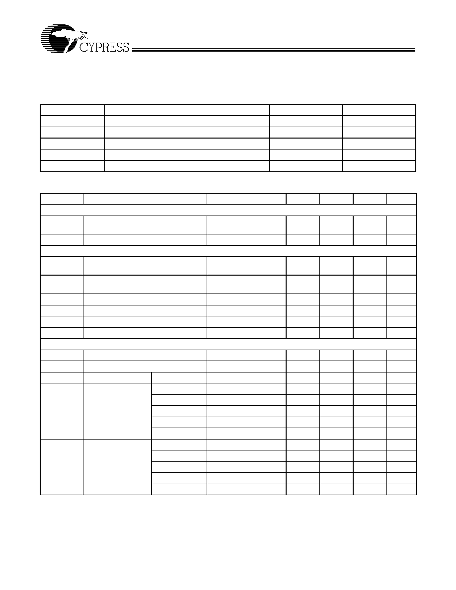
Absolute Maximum Ratings
Stresses greater than those listed in this table may cause per-
manent damage to the device. These represent a stress rating
only. Operation of the device at these or any other conditions
above those specified in the operating sections of this specifi-
cation is not implied. Maximum conditions for extended peri-
ods may affect reliability.
Parameter
Description
Rating
Unit
V
DD
, V
IN
Voltage on any pin with respect to GND
0.5 to +7.0
V
T
STG
Storage Temperature
65 to +150
°C
T
A
Operating Temperature
0 to +70
°C
T
B
Ambient Temperature under Bias
55 to +125
°C
ESD
PROT
Input ESD Protection
2 (min.)
kV
DC Electrical Characteristics:
T
A
= 0°C to +70°C, V
DDQ3
= 3.3V±5%, V
DDQ2
= 2.5V±5%
Parameter
Description
Test Condition
Min.
Typ.
Max.
Unit
Supply Current
I
DDQ3
3.3V Supply Current
CPUCLK =100 MHz
Outputs Loaded
[3]
120
mA
I
DDQ3
2.5V Supply Current
60
mA
Logic Inputs
V
IL
Input Low Voltage
GND
0.3
0.8
V
V
IH
Input High Voltage
2.0
V
DD
+
0.3
V
I
IL
Input Low Current
[4]
25
µA
I
IH
Input High Current
[4]
10
µA
I
IL
Input Low Current (SEL100/66#)
5
µA
I
IH
Input High Current (SEL100/66#)
5
µA
Clock Outputs
V
OL
Output Low Voltage
I
OL
= 1 mA
50
mV
V
OH
Output High Voltage
I
OH
= 1 mA
3.1
V
V
OH
Output High Voltage
(CPU, APIC)
I
OH
= 1 mA
2.2
V
I
OL
Output Low Current
CPU0:3
V
OL
= 1.25V
27
57
97
mA
PCI_F, PCI1:7
V
OL
= 1.5V
20.5
53
139
mA
APIC0:1
V
OL
= 1.25V
40
85
140
mA
REF0:2
V
OL
= 1.5V
25
37
76
mA
48MHz 0:1
V
OL
= 1.5V
25
37
76
mA
I
OH
Output High Current
CPU0:3
V
OL
= 1.25V
25
55
97
mA
PCI_F, PCI1:7
V
OL
= 1.5V
31
55
189
mA
APIC0:1
V
OL
= 1.25V
40
87
155
mA
REF0:2
V
OL
= 1.5V
27
44
94
mA
48MHz 0:1
V
OL
= 1.5V
27
44
94
mA
Notes:
3.
All clock outputs loaded with maximum lump capacitance test load specified in the AC Electrical Characteristics section.
4.
W48S101-04 logic inputs have internal pull-up devices, except SEL100/66#.
W48S101-04
PRELIMINARY
9
AC Electrical Characteristics
T
A
= 0°C to +70°C, V
DDQ3
= 3.3V±5%,V
DDQ2
= 2.5V± 5%, f
XTL
= 14.31818 MHz
AC clock parameters are tested and guaranteed over stated operating conditions using the stated lump capacitive load at the
clock output; Spread Spectrum clocking is disabled.
Notes:
5.
X1 input threshold voltage (typical) is V
DD
/2.
6.
The W48S101-04 contains an internal crystal load capacitor between pin X1 and ground and another between pin X2 and ground. Total load placed on crystal
is 14 pF; this includes typical stray capacitance of short PCB traces to crystal.
7.
X1 input capacitance is applicable when driving X1 with an external clock source (X2 is left unconnected).
Crystal Oscillator
V
TH
X1 Input Threshold Voltage
[5]
1.5
V
C
LOAD
Load Capacitance, as seen by
External Crystal
[6]
14
pF
C
IN,X1
X1 Input Capacitance
[7]
Pin X2 unconnected
28
pF
Pin Capacitance/Inductance
C
IN
Input Pin Capacitance
Except X1 and X2
5
pF
C
OUT
Output Pin Capacitance
6
pF
L
IN
Input Pin Inductance
7
nH
DC Electrical Characteristics:
T
A
= 0°C to +70°C, V
DDQ3
= 3.3V±5%, V
DDQ2
= 2.5V±5% (continued)
Parameter
Description
Test Condition
Min.
Typ.
Max.
Unit
CPU Clock Outputs, CPU0:3 (Lump Capacitance Test Load = 20 pF)
Parameter
Description
Test Condition/Comments
CPU = 66.8 MHz
CPU = 100 MHz
Unit
Min.
Typ. Max.
Min.
Typ.
Max.
t
P
Period
Measured on rising edge at 1.25V
15
15.5
10
10.5
ns
t
H
High Time
Duration of clock cycle above 2.0V
5.2
3.0
ns
t
L
Low Time
Duration of clock cycle below 0.4V
5.0
2.8
ns
t
R
Output Rise Edge Rate Measured from 0.4V to 2.0V
1
4
1
4
V/ns
t
F
Output Fall Edge Rate
Measured from 2.0V to 0.4V
1
4
1
4
V/ns
t
D
Duty Cycle
Measured on rising and falling edge at
1.25V
45
55
45
55
%
t
JC
Jitter, Cycle-to-Cycle
Measured on rising edge at 1.25V. Max-
imum difference of cycle time between
two adjacent cycles.
200
250
ps
t
SK
Output Skew
Measured on rising edge at 1.25V
175
175
ps
f
ST
Frequency Stabiliza-
tion from Power-up
(cold start)
Assumes full supply voltage reached
within 1 ms from power-up. Short cycles
exist prior to frequency stabilization.
3
3
ms
Z
o
AC Output Impedance
Average value during switching transi-
tion. Used for determining series termi-
nation value.
20
20
W48S101-04
PRELIMINARY
10
PCI Clock Outputs, PCI1:7 and PCI_F (Lump Capacitance Test Load = 30 pF
Parameter
Description
Test Condition/Comments
CPU = 66.8/100 MHz
Unit
Min.
Typ.
Max.
t
P
Period
Measured on rising edge at 1.5V
30
ns
t
H
High Time
Duration of clock cycle above 2.4V
12
ns
t
L
Low Time
Duration of clock cycle below 0.4V
12
ns
t
R
Output Rise Edge Rate
Measured from 0.4V to 2.4V
1
4
V/ns
t
F
Output Fall Edge Rate
Measured from 2.4V to 0.4V
1
4
V/ns
t
D
Duty Cycle
Measured on rising and falling edge at 1.5V
45
55
%
t
JC
Jitter, Cycle-to-Cycle
Measured on rising edge at 1.5V. Maximum
difference of cycle time between two adjacent cycles.
250
ps
t
SK
Output Skew
Measured on rising edge at 1.5V
500
ps
t
O
CPU to PCI Clock Skew
Covers all CPU/PCI outputs. Measured on rising
edge at 1.5V. CPU leads PCI output.
1.5
4
ns
f
ST
Frequency Stabilization
from Power-up (cold
start)
Assumes full supply voltage reached within 1 ms
from power-up. Short cycles exist prior to frequency
stabilization.
3
ms
Z
o
AC Output Impedance
Average value during switching transition. Used for
determining series termination value.
30
APIC0:1 Clock Output (Lump Capacitance Test Load = 20 pF)
Parameter
Description
Test Condition/Comments
CPU = 66.8/100 MHz
Unit
Min.
Typ.
Max.
f
Frequency, Actual
Frequency generated by crystal oscillator
14.31818
MHz
t
R
Output Rise Edge Rate
Measured from 0.4V to 2.0V
1
4
V/ns
t
F
Output Fall Edge Rate
Measured from 2.0V to 0.4V
1
4
V/ns
t
D
Duty Cycle
Measured on rising and falling edge at 1.25V
45
55
%
f
ST
Frequency Stabilization
from Power-up (cold start)
Assumes full supply voltage reached within
1 ms from power-up. Short cycles exist prior to
frequency stabilization.
1.5
ms
Z
o
AC Output Impedance
Average value during switching transition. Used
for determining series termination value.
15
REF0:2 Clock Output (Lump Capacitance Test Load = 20 pF)
Parameter
Description
Test Condition/Comments
CPU = 66.8/100 MHz
Unit
Min.
Typ.
Max.
f
Frequency, Actual
Frequency generated by crystal oscillator
14.318
MHz
t
R
Output Rise Edge Rate
Measured from 0.4V to 2.4V
0.5
2
V/ns
t
F
Output Fall Edge Rate
Measured from 2.4V to 0.4V
0.5
2
V/ns
t
D
Duty Cycle
Measured on rising and falling edge at 1.5V
45
55
%
f
ST
Frequency Stabilization from
Power-up (cold start)
Assumes full supply voltage reached within
1 ms from power-up. Short cycles exist prior to
frequency stabilization.
3
ms
Z
o
AC Output Impedance
Average value during switching transition. Used
for determining series termination value.
40
W48S101-04
PRELIMINARY
11
Document #: 38-00853
48MHz0:1 Clock Output (Lump Capacitance Test Load = 20 pF = 66.6/100 MHz)
Parameter
Description
Test Condition/Comments
CPU = 66.8/100 MHz
Unit
Min.
Typ.
Max.
f
Frequency, Actual
Determined by PLL divider ratio (see m/n below)
48.008
MHz
f
D
Deviation from 48 MHz
(48.008 48)/48
+167
ppm
m/n
PLL Ratio
(14.31818 MHz x 57/17 = 48.008 MHz)
57/17
t
R
Output Rise Edge Rate
Measured from 0.4V to 2.4V
0.5
2
V/ns
t
F
Output Fall Edge Rate
Measured from 2.4V to 0.4V
0.5
2
V/ns
t
D
Duty Cycle
Measured on rising and falling edge at 1.5V
45
55
%
f
ST
Frequency Stabilization
from Power-up (cold start)
Assumes full supply voltage reached within 1 ms
from power-up. Short cycles exist prior to fre-
quency stabilization.
3
ms
Z
o
AC Output Impedance
Average value during switching transition. Used
for determining series termination value.
40
Ordering Information
Ordering Code
Freq. Mask
Code
Package
Name
Package Type
W48S101
-04
H
48-pin SSOP (300 mils)
W48S101-04
PRELIMINARY
© Cypress Semiconductor Corporation, 1999. The information contained herein is subject to change without notice. Cypress Semiconductor Corporation assumes no responsibility for the use
of any circuitry other than circuitry embodied in a Cypress Semiconductor product. Nor does it convey or imply any license under patent or other rights. Cypress Semiconductor does not authorize
its products for use as critical components in life-support systems where a malfunction or failure may reasonably be expected to result in significant injury to the user. The inclusion of Cypress
Semiconductor products in life-support systems application implies that the manufacturer assumes all risk of such use and in doing so indemnifies Cypress Semiconductor against all charges.
Package Diagram
48-Pin Small Shrink Outline Package (SSOP, 300 mils)
Summary of nominal dimensions in inches:
Body Width: 0.296
Lead Pitch: 0.025
Body Length: 0.625
Body Height: 0.102