DS11108 Rev. 14 - 2
1 of 3
BC846A-BC848C
BC846A - BC848C
NPN SURFACE MOUNT SMALL SIGNAL TRANSISTOR
Features
Maximum Ratings
@ T
A
= 25∞C unless otherwise specified
Characteristic
Symbol
Value
Unit
Collector-Base Voltage
BC846
BC847
BC848
V
CBO
80
50
30
V
Collector-Emitter Voltage
BC846
BC847
BC848
V
CEO
65
45
30
V
Emitter-Base Voltage
BC846, BC847
BC848
V
EBO
6.0
5.0
V
Collector Current
I
C
100
mA
Peak Collector Current
I
CM
200
mA
Peak Emitter Current
I
EM
200
mA
Power Dissipation (Note 1)
P
d
300
mW
Thermal Resistance, Junction to Ambient Air (Note 1)
R
qJA
417
∞C/W
Operating and Storage Temperature Range
T
j
, T
STG
-65 to +150
∞C
∑
Ideally Suited for Automatic Insertion
∑
Complementary PNP Types Available
(BC856-BC858)
∑
For Switching and AF Amplifier Applications
Marking Code (Note 2)
Type
Marking
Type
Marking
BC846A
1A, K1Q
BC847C
1G, K1M
BC846B
1B, K1R
BC848A
1J, K1J, K1E, K1Q
BC847A
1E, K1E, K1Q
BC848B
1K, K1K, K1F, K1R
BC847B
1F, K1F, K1R
BC848C
1L, K1L, K1M
∑
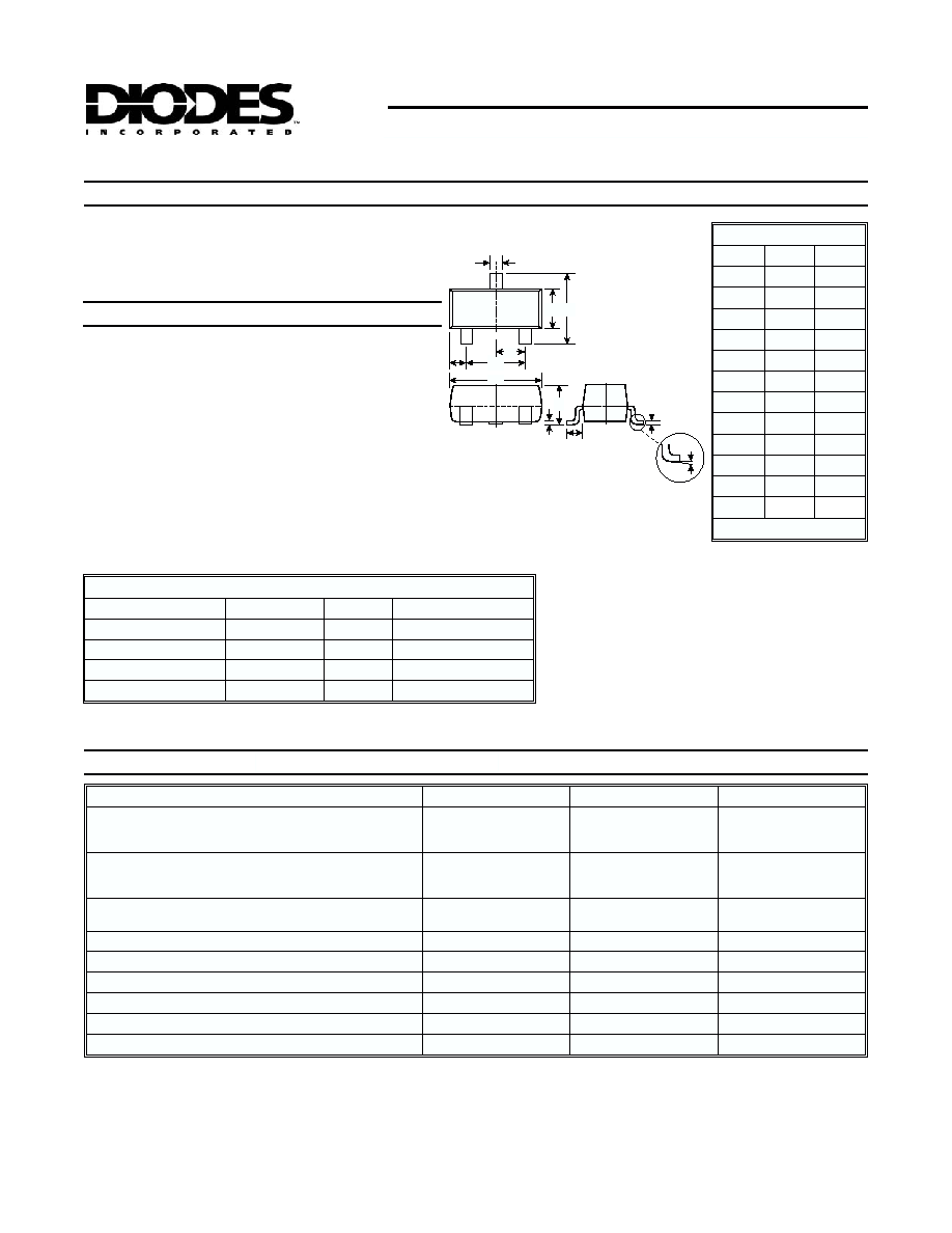
Case: SOT-23, Molded Plastic
∑
Case material - UL Flammability Rating
Classification 94V-0
∑
Moisture sensitivity: Level 1 per J-STD-020A
∑
Terminals: Solderable per MIL-STD-202,
Method 208
∑
Pin Connections: See Diagram
∑
Marking Codes (See Table Below & Diagram
on Page 3)
∑
Ordering & Date Code Information: See Page 3
∑
Approx. Weight: 0.008 grams
Mechanical Data
A
E
J
L
TOP VIEW
M
B C
H
G
D
K
C
B
E
Notes:
1. Device mounted on FR-4 PCB, 1 inch x 0.85 inch x 0.062 inch; pad layout as shown on Diodes Inc. suggested pad layout
document AP02001, which can be found on our website at http://www.diodes.com/datasheets/ap02001.pdf
2. Current gain subgroup "C" is not available for BC846.
SOT-23
Dim
Min
Max
A
0.37
0.51
B
1.20
1.40
C
2.30
2.50
D
0.89
1.03
E
0.45
0.60
G
1.78
2.05
H
2.80
3.00
J
0.013
0.10
K
0.903
1.10
L
0.45
0.61
M
0.85
0.80
a
0
∞
8
∞
All Dimensions in mm

DS11108 Rev. 14 - 2
2 of 3
BC846A-BC848C
Electrical Characteristics
@ T
A
= 25∞C unless otherwise specified
Characteristic
Symbol
Min
Typ
Max
Unit
Test Condition
Collector-Base Breakdown Voltage (Note 3) BC846
BC847
BC848
V
(BR)CBO
80
50
30
--
--
--
--
--
--
V
I
C
= 10
mA, I
B
= 0
Collector-Emitter Breakdown Voltage (Note 3) BC846
BC847
BC848
V
(BR)CEO
65
45
30
--
--
--
--
--
--
V
I
C
= 10mA, I
B
= 0
Emitter-Base Breakdown Voltage BC846, BC847
(Note 3) BC848
V
(BR)EBO
6
5
--
--
V
I
E
= 1
mA, I
C
= 0
H-Parameters
Small Signal Current Gain
Current Gain Group A
B
C
Input Impedance
Current Gain Group A
B
C
Output Admittance
Current Gain Group A
B
C
Reverse Voltage Transfer Ratio
A
Current Gain Group B
C
h
fe
h
fe
h
fe
h
ie
h
ie
h
ie
h
oe
h
oe
h
oe
h
re
h
re
h
re
--
--
--
--
--
--
--
--
--
--
--
--
220
330
600
2.7
4.5
8.7
18
30
60
1.5x10
-4
2x10
-4
3x10
-4
--
--
--
--
--
--
--
--
--
--
--
--
--
--
--
k
W
k
W
k
W
µS
µS
µS
--
--
--
V
CE
= 5.0V, I
C
= 2.0mA,
f = 1.0kHz
DC Current Gain
Current Gain Group A
B
(Note 3) C
h
FE
110
200
420
180
290
520
220
450
800
--
V
CE
= 5.0V, I
C
= 2.0mA
Collector-Emitter Saturation Voltage (Note 3)
V
CE(SAT)
--
90
200
250
600
mV
I
C
= 10mA, I
B
= 0.5mA
I
C
= 100mA, I
B
= 5.0mA
Base-Emitter Saturation Voltage (Note 3)
V
BE(SAT)
--
700
900
--
mV
I
C
= 10mA, I
B
= 0.5mA
I
C
= 100mA, I
B
= 5.0mA
Base-Emitter Voltage (Note 3)
V
BE(ON)
580
--
660
--
700
770
mV
V
CE
= 5.0V, I
C
= 2.0mA
V
CE
= 5.0V, I
C
= 10mA
Collector-Cutoff Current (Note 3)
BC846
BC847
BC848
I
CES
I
CES
I
CES
I
CBO
I
CBO
--
--
--
--
--
--
--
--
--
--
15
15
15
15
5.0
nA
nA
nA
nA
µA
V
CE
= 80V
V
CE
= 50V
V
CE
= 30V
V
CB
= 40V
V
CB
= 30V, T
A
= 150∞C
Gain Bandwidth Product
f
T
100
300
--
MHz
V
CE
= 5.0V, I
C
= 10mA,
f = 100MHz
Collector-Base Capacitance
C
CBO
--
3.0
--
pF
V
CB
= 10V, f = 1.0MHz
Noise Figure
NF
--
2
10
dB
V
CE
= 5V, I
C
= 200µA,
R
S
= 2.0k
W,
f = 1.0kHz,
Df = 200Hz
Notes:
3. Short duration pulse test used to minimize self-heating effect.
DS11108 Rev. 14 - 2
3 of 3
BC846A-BC848C
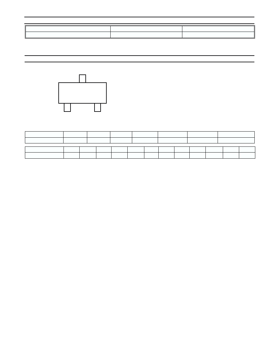
Month
Jan
Feb
March
Apr
May
Jun
Jul
Aug
Sep
Oct
Nov
Dec
Code
1
2
3
4
5
6
7
8
9
O
N
D
Year
1998
1999
2000
2001
2002
2003
2004
Code
J
K
L
M
N
P
R
Date Code Key
XXX = Product Type Marking Code (See Page 1), e.g. K1Q or 1A = BC846A
YM = Date Code Marking
Y = Year ex: N = 2002
M = Month ex: 9 = September
XXX
YM
Marking Information
Notes:
4. For Packaging Details, go to our website at http://www.diodes.com/datasheets/ap02007.pdf.
* xx = device type, e.g. BC846A-7.
Device
Packaging
Shipping
BC84xx-7*
SOT-23
3000/Tape & Reel
Ordering Information
(Note 4)