
DS16001 Rev. D-2
1 of 2
DL4001-DL4007
∑
Glass Passivated Junction
∑
High Current Capability
∑
Low Forward Voltage Drop
∑
High Reliability and Low Leakage
∑
For Surface Mount Application
∑
Plastic Material - UL Flammability
Classification Rating 94V-0
Features
DL4001 - DL4007
1.0A SURFACE MOUNT GLASS PASSIVATED RECTIFIER
Notes:
1. Measured at 1.0MHz and applied reverse voltage of 4.0 volts.
Single phase, half wave, 60Hz, resistive or inductive load.
For capacitive load, derate current by 20%.
Maximum Ratings and Electrical Characteristics
@ T
A
= 25
∞C unless otherwise specified
Mechanical Data
∑
Case: MELF, Plastic
∑
Terminals: Solderable per MIL-STD-202,
Method 208
∑
Polarity: Cathode band
∑
Approx Weight: 0.25 grams
∑
Mounting Position: Any
MELF
Dim
Min
Max
A
4.80
5.20
B
2.40
2.60
C
0.55 Nominal
All Dimensions in mm
C
A
B
Characteristic
Symbol
DL
4001
DL
4002
DL
4003
DL
4004
DL
4005
DL
4006
DL
4007
Unit
Peak Repetitive Reverse Voltage
Working Peak Reverse Voltage
DC Blocking Voltage
V
RRM
V
RWM
V
R
50
100
200
400
600
800
1000
V
RMS Reverse Voltage
V
R(RMS)
35
71
141
283
424
566
707
V
Maximum Average Forward Rectified
Current @ Terminal Temp
@ T
T
= 75
∞C
I
O
1.0
A
Peak Forward Surge Current 8.3ms single half sine-wave
Superimposed on Rated Load (JEDEC Method)
I
FSM
30
A
Maximum Forward Voltage
@ I
F
= 1.0A
V
F
1.1
V
Maximum dc Reverse Current
@ T
A
= 25
∞C
Rated DC Blocking Voltage
@ T
A
= 100
∞C
I
R
5.0
50
mA
Typical Thermal Resistance, Junction to Ambient Air
R
qJA
50
K/W
Typical Junction Capacitance (Note 1)
C
j
15
pF
Operating and Storage Temperature Range
T
j,
T
STG
-55 to +150
∞C
DS16001 Rev. D-2
2 of 2
DL4001-DL4007
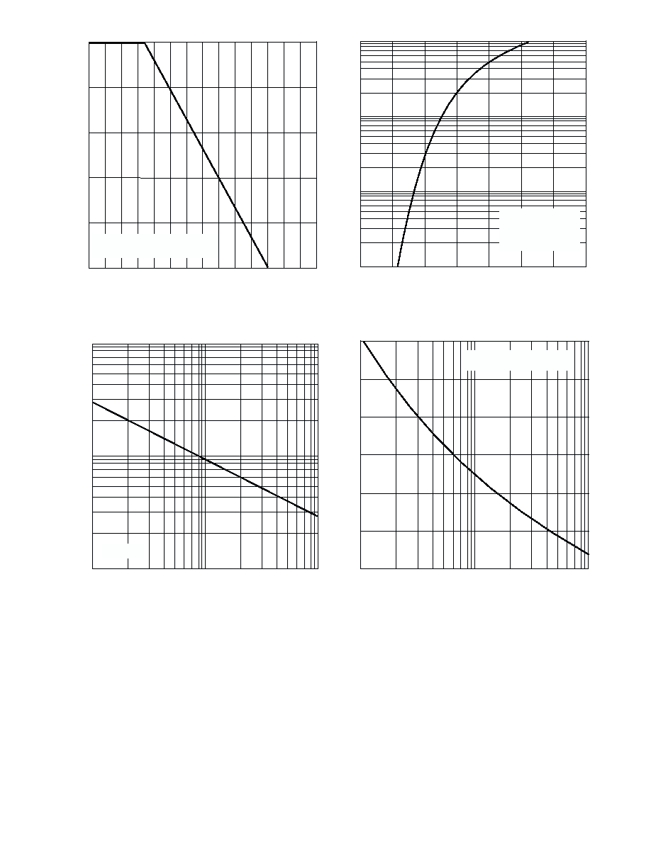
40
60
80
100
120 140
160
180
0
.2
.4
.6
.8
1.0
I
,
A
VERAGE
OUTPUT
CURRENT
(A)
O
T , AMBIENT TEMPERATURE (∫C)
Fig. 1 Forward Current Derating Curve
A
Single phase half wave
60 Hz resistive or inductive load
5
10
15
20
25
30
1
10
100
PEAK
FWD
S
UR
G
E
C
URRENT
(
A
)
NUMBER OF CYCLES AT 60 Hz
Fig. 4 Max Non-Repetitive Peak Fwd Surge Current
8.3ms Single Half Sine-Wave
JEDEC Method
0
1
10
100
1
10
100
C
,
JUNCTI
O
N
CAP
ACIT
ANCE
(pF)
j
V , REVERSE VOLTAGE (V)
Fig. 3 Typical Junction Capacitance
R
T = 25∫C
J
0.01
0.1
1.0
I
,
INST
ANT
ANEOUS
FWD
CURRENT
(A)
F
V , INSTANTANEOUS FORWARD VOLTAGE (V)
Fig. 2 Typical Forward Characteristics
F
10
0.4
0.6
0.8
1.0
1.2
1.4
1.6
1.8
T= 25∫C
Pulse Width = 300 ms
1% duty cycle
j