
DS30563 Rev. 2 - 0
1 of 4
MMDT2222V
www.diodes.com
„
Diodes Incorporated
∑
Epitaxial Planar Die Construction
∑
Complementary PNP Type Available
(MMDT2907V)
∑
Ultra-Small Surface Mount Package
∑
Lead Free By Design/RoHS Compliant (Note 1)
∑
"Green" Device (Note 2)
Features
Maximum Ratings
@ T
A
= 25
∞C unless otherwise specified
A
M
L
B C
H
K
G
D
Mechanical Data
MMDT2222V
DUAL NPN SMALL SIGNAL SURFACE MOUNT TRANSISTOR
Characteristic
Symbol
Value
Unit
Collector-Base Voltage
V
CBO
75
V
Collector-Emitter Voltage
V
CEO
40
V
Emitter-Base Voltage
V
EBO
6.0
V
Collector Current - Continuous (Note 3)
I
C
600
mA
Operating and Storage and Temperature Range
T
j
, T
STG
-55 to +150
∞C
SOT-563
Dim
Min
Max
Typ
A
0.15
0.30
0.25
B
1.10
1.25
1.20
C
1.55
1.70
1.60
D
0.50
G
0.90
1.10
1.00
H
1.50
1.70
1.60
K
0.56
0.60
0.60
L
0.10
0.30
0.20
M
0.10
0.18
0.11
All Dimensions in mm
C
1
B
2
E
2
C
2
E
1
B
1
ADVANCE
INFORMATION
Notes:
1. No purposefully added lead.
2. Diodes Inc.'s "Green" policy can be found on our website at http://www.diodes.com/products/lead_free/index.php.
3. Device mounted on FR-4 PCB, 1 inch x 0.85 inch x 0.062 inch; pad layout as shown on Diodes Inc. suggested pad layout
document AP02001, which can be found on our website at http://www.diodes.com/datasheets/ap02001.pdf.
∑
Case: SOT-563, Molded Plastic
∑
Case Material: Molded Plastic, "Green" Molding
Compound. UL Flammability Classification Rating 94V-0
∑
Moisture sensitivity: Level 1 per J-STD-020C
∑
Terminal Connections: See Diagram
∑
Terminals: Finish
æ Matte Tin annealed over Alloy 42
leadframe. Solderable per MIL-STD-202, Method 208
∑
Polarity: See Diagrams Below
∑
Marking & Type Code Information: See Last Page
∑
Ordering Information: See Last Page
∑
Weight: 0.003 grams (approx.)
Thermal Characteristics
@ T
A
= 25
∞C unless otherwise specified
Characteristic
Symbol
Value
Unit
Power Dissipation (Note 3)
P
d
150
mW
Thermal Resistance, Junction to Ambient (Note 3)
R
qJA
833
∞C/W

DS30563 Rev. 2 - 0
2 of 4
MMDT2222V
www.diodes.com
Electrical Characteristics
@ T
A
= 25
∞C unless otherwise specified
Characteristic
Symbol
Min
Max
Unit
Test Condition
OFF CHARACTERISTICS (Note 4)
Collector-Base Breakdown Voltage
V
(BR)CBO
75
æ
V
I
C
= 10
mA, I
E
= 0
Collector-Emitter Breakdown Voltage
V
(BR)CEO
40
æ
V
I
C
= 10mA, I
B
= 0
Emitter-Base Breakdown Voltage
V
(BR)EBO
6.0
æ
V
I
E
= 10
mA, I
C
= 0
Collector Cutoff Current
I
CBO
æ
10
nA
mA
V
CB
= 60V, I
E
= 0
V
CB
= 60V, I
E
= 0, T
A
= 150
∞C
Collector Cutoff Current
I
CEX
æ
10
nA
V
CE
= 60V, V
EB(OFF)
= 3.0V
Emitter Cutoff Current
I
EBO
æ
10
nA
V
EB
= 3.0V, I
C
= 0
Base Cutoff Current
I
BL
æ
20
nA
V
CE
= 60V, V
EB(OFF)
= 3.0V
ON CHARACTERISTICS (Note 4)
DC Current Gain
h
FE
35
50
75
100
40
50
35
æ
æ
æ
300
æ
æ
æ
æ
I
C
= 100
mA, V
CE
= 10V
I
C
= 1.0mA, V
CE
= 10V
I
C
= 10mA, V
CE
= 10V
I
C
= 150mA, V
CE
= 10V
I
C
= 500mA, V
CE
= 10V
I
C
= 10mA, V
CE
= 10V, T
A
= -55
∞C
I
C
= 150mA, V
CE
= 1.0V
Collector-Emitter Saturation Voltage
V
CE(SAT)
æ
0.3
1.0
V
I
C
= 150mA, I
B
= 15mA
I
C
= 500mA, I
B
= 50mA
Base-Emitter Saturation Voltage
V
BE(SAT)
0.6
æ
1.2
2.0
V
I
C
= 150mA, I
B
= 15mA
I
C
= 500mA, I
B
= 50mA
SMALL SIGNAL CHARACTERISTICS
Output Capacitance
C
obo
æ
8
pF
V
CB
= 10V, f = 1.0MHz, I
E
= 0
Input Capacitance
C
ibo
--
25
pF
V
EB
= 0.5V, f = 1.0MHz, I
C
= 0
Current Gain-Bandwidth Product
f
T
300
æ
MHz
V
CE
= 20V, I
C
= 20mA,
f = 100MHz
Noise Figure
NF
æ
4.0
dB
V
CE
= 10V, I
C
= 100
mA,
R
S
= 1.0k
W, f = 1.0kHz
SWITCHING CHARACTERISTICS
Delay Time
t
d
æ
10
ns
V
CC
= 30V, I
C
= 150mA,
V
BE(off)
= - 0.5V, I
B1
= 15mA
Rise Time
t
r
æ
25
ns
Storage Time
t
s
æ
225
ns
V
CC
= 30V, I
C
= 150mA,
I
B1
= I
B2
= 15mA
Fall Time
t
f
æ
60
ns
ADVANCE
INFORMATION
Notes:
4. Short duration test pulse used to minimize self-heating effect.
DS30563 Rev. 2 - 0
3 of 4
MMDT2222V
www.diodes.com
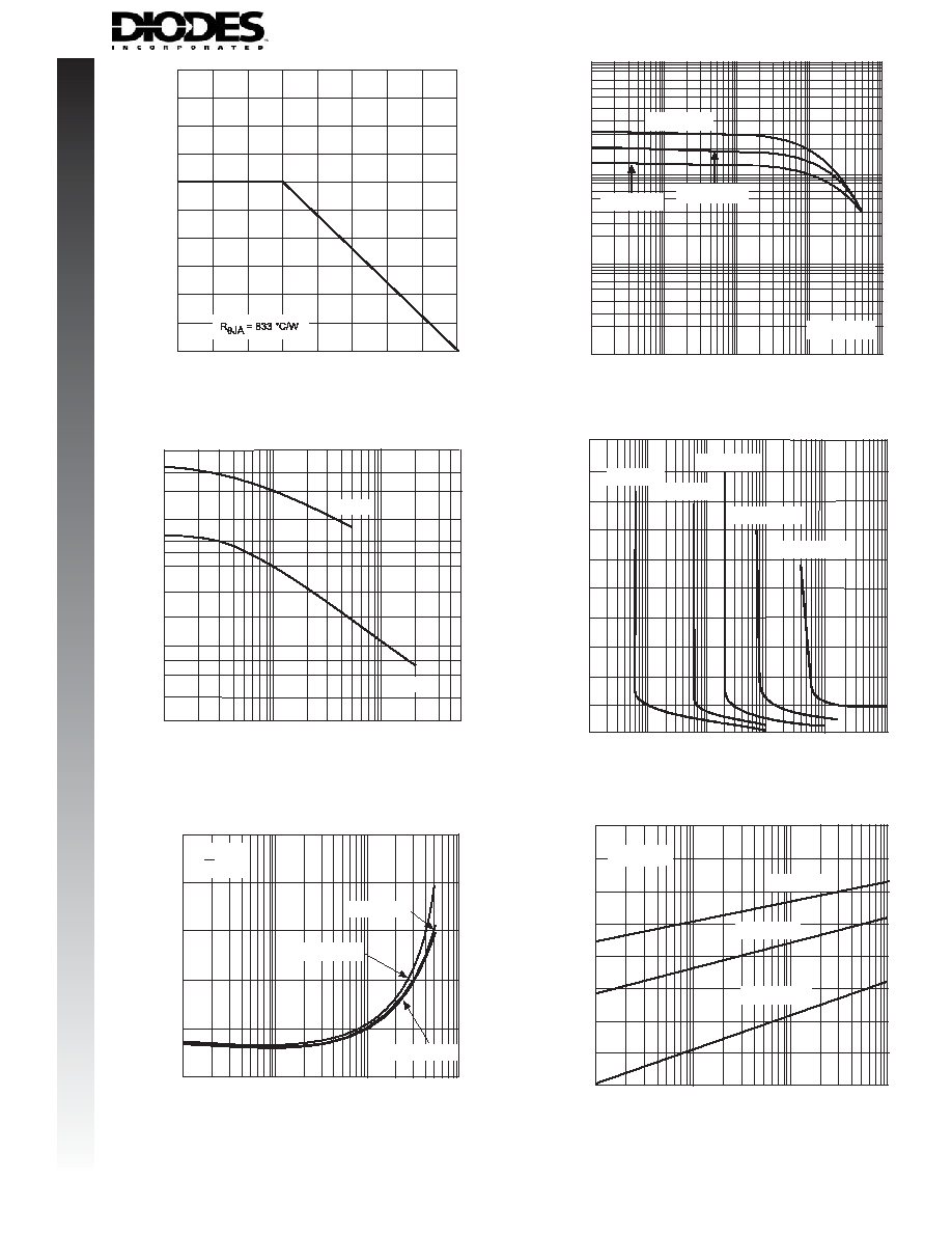
-50
0
50
100
150
250
200
150
50
100
0
T , AMBIENT TEMPERATURE ( C)
Fig. 1, Derating Curve - Total
A
∞
P,
P
O
WER
D
ISSIP
A
T
I
O
N
(mW)
d
ADVANCE
INFORMATION
1
10
1000
100
0.1
1
10
1000
100
h
,
DC
CURRENT
GAIN
FE
I , COLLECTOR CURRENT (mA)
Fig. 2 Typical DC Current Gain vs
Collector Current
C
T = -25∞C
A
T = +25∞C
A
T = 125∞C
A
V
= 1.0V
CE
0.001
0.01
1
10
0.1
100
0
0.2
0.4
0.6
0.8
1.0
1.2
1.4
1.6
1.8
2.0
I , BASE CURRENT (mA)
Fig. 4 Typical Collector Saturation Region
B
V,
C
O
LLECT
O
R-EMITTER
V
O
L
T
AGE
(V)
CE
I = 1mA
C
I = 10mA
C
I = 30mA
C
I = 100mA
C
I = 300mA
C
1.0
5.0
20
10
30
0.1
10
1.0
50
CAP
A
CIT
A
NCE
(pF)
REVERSE VOLTS (V)
Fig. 3 Typical Capacitance
Cobo
Cibo
1
0.1
10
100
V
,
BASE
EMITTER
V
O
L
T
AGE
(V)
BE(ON)
I , COLLECTOR CURRENT (mA)
Fig. 6 Base Emitter Voltage vs. Collector Current
C
0.2
0.3
0.4
0.6
0.5
0.8
0.7
1.0
0.9
V
= 5V
CE
T = 25∞C
A
T = -50∞C
A
T = 150∞C
A
1
10
100
1000
V,
C
O
LLECT
O
RT
O
EMITTER
SA
TURA
TION
VOL
T
AGE
(V)
CE(SA
T)
I , COLLECTOR CURRENT (mA)
Fig. 5 Collector Emitter Saturation Voltage
vs. Collector Current
C
T = 25∞C
A
T = -50∞C
A
T = 150∞C
A
0
0.1
0.2
0.3
0.4
0.5
I
C
I
B
= 10
DS30563 Rev. 2 - 0
4 of 4
MMDT2222V
www.diodes.com
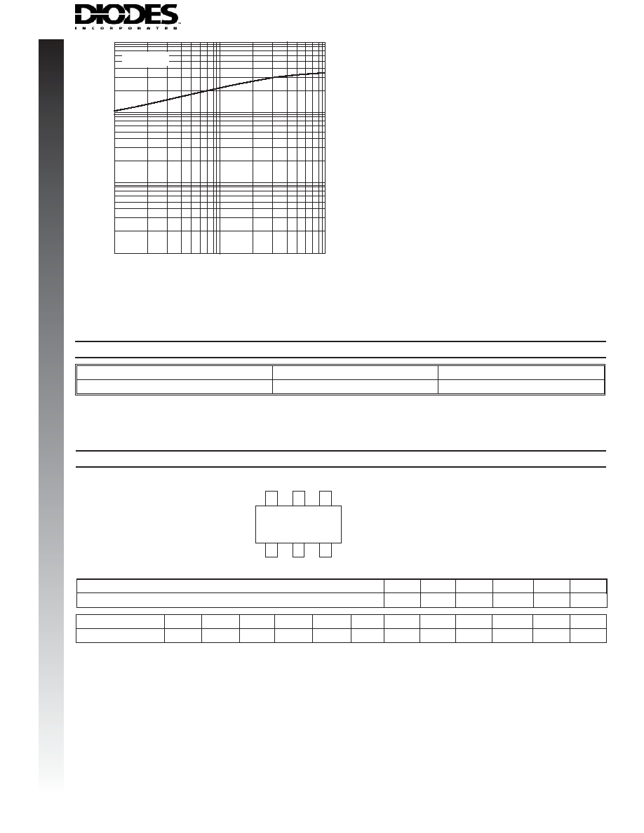
1
10
100
1000
1
10
100
I , COLLECTOR CURRENT (mA)
Fig. 7 Gain Bandwidth Product vs. Collector Current
C
f
,
GAIN
BANDWIDTH
PR
O
DUCT
(MHz)
T
V
= 5V
CE
ADVANCE
INFORMATION
Ordering Information
Device
Packaging
Shipping
MMDT2222V-7
SOT-563
3000/Tape & Reel
Notes:
5. For Packaging Details, go to our website at http://www.diodes.com/datasheets/ap02007.pdf.
Marking Information
KAT YM
KAT = Product Type Marking Code
YM = Date Code Marking
Y = Year ex: R = 2004
M = Month ex: 9 = September
Date Code Key
Year
2004
2005
2006
2007
2008
2009
Code
R
S
T
U
V
W
(Note 5)
Month
Jan
Feb
March
Apr
May
Jun
Jul
Aug
Sep
Oct
Nov
Dec
Code
1
2
3
4
5
6
7
8
9
O
N
D