Pb
Lead-free
DS30467 Rev. 6 - 2
1 of 4
MMDT3906V
www.diodes.com
„
Diodes Incorporated
∑
Epitaxial Planar Die Construction
∑
Ideal for Low Power Amplification and Switching
∑
Ultra-Small Surface Mount Package
∑
Lead Free By Design/RoHS Compliant (Note 1)
∑
Qualified to AEC-Q101 Standards for High Reliability
Features
Maximum Ratings
@ T
A
= 25
∞C unless otherwise specified
A
M
L
B C
H
K
G
D
C
1
B
2
E
2
C
2
E
1
B
1
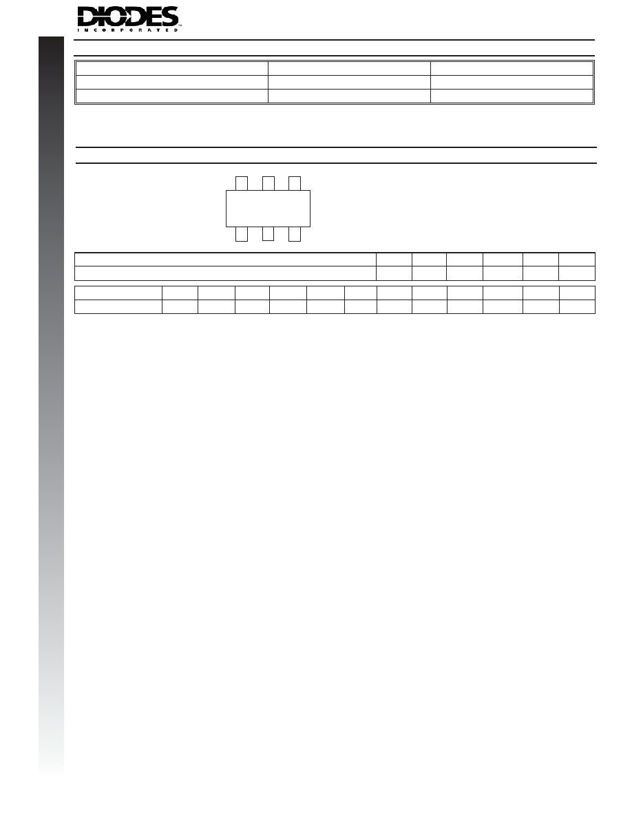
Mechanical Data
∑
Case: SOT-563
∑
Case Material: Molded Plastic. UL Flammability
Classification Rating 94V-0
∑
Moisture sensitivity: Level 1 per J-STD-020C
∑
Terminal Connections: See Diagram
∑
Terminals: Finish - Matte Tin annealed over Alloy 42
leadframe. Solderable per MIL-STD-202, Method 20
∑
Terminals: Lead bearing terminal plating available. See
Ordering information Page 4, Note 6
∑
Marking & Type Code Information: See Last Page
∑
Ordering Information: See Last Page
∑
Weight: 0.003 grams (approximate)
MMDT3906V
DUAL PNP SMALL SIGNAL SURFACE MOUNT
TRANSISTOR
Characteristic
Symbol
Value
Unit
Collector-Base Voltage
V
CBO
-40
V
Collector-Emitter Voltage
V
CEO
-40
V
Emitter-Base Voltage
V
EBO
-5.0
V
Collector Current - Continuous
I
C
-200
mA
Power Dissipation (Note 3)
P
d
150
mW
Thermal Resistance, Junction to Ambient
R
qJA
833
∞C/W
Operating and Storage and Temperature Range
T
j
, T
STG
-55 to +150
∞C
SOT-563
Dim
Min
Max
Typ
A
0.15
0.30
0.25
B
1.10
1.25
1.20
C
1.55
1.70
1.60
D
0.50
G
0.90
1.10
1.00
H
1.50
1.70
1.60
K
0.56
0.60
0.60
L
0.10
0.30
0.20
M
0.10
0.18
0.11
All Dimensions in mm
SEE NOTE 2
C
1
B
2
E
2
C
2
E
1
B
1
NEW
P
RODUCT
Notes:
1. No purposefully added lead.
2. Package is non-polarized. Parts may be on reel in orientation illustrated, 180
∞ rotated, or mixed (both ways).
3. Device mounted on FR-4 PCB, 1 inch x 0.85 inch x 0.062 inch; pad layout as shown on Diodes Inc. suggested pad layout
document AP02001, which can be found on our website at http://www.diodes.com/datasheets/ap02001.pdf.
Thermal Characteristics
@ T
A
= 25
∞C unless otherwise specified
Characteristic
Symbol
Value
Unit
Power Dissipation (Note 3)
P
d
150
mW
Thermal Resistance, Junction to Ambient
R
qJA
833
∞C/W
SPICE MODEL: MMDT3906V

DS30467 Rev. 6 - 2
2 of 4
MMDT3906V
www.diodes.com
Electrical Characteristics
@ T
A
= 25
∞C unless otherwise specified
Characteristic
Symbol
Min
Max
Unit
Test Condition
OFF CHARACTERISTICS (Note 4)
Collector-Base Breakdown Voltage
V
(BR)CBO
-40
æ
V
I
C
= -10
mA, I
E
= 0
Collector-Emitter Breakdown Voltage
V
(BR)CEO
-40
æ
V
I
C
= -1.0mA, I
B
= 0
Emitter-Base Breakdown Voltage
V
(BR)EBO
-5.0
æ
V
I
E
= -10
mA, I
C
= 0
Collector Cutoff Current
I
CEX
æ
-50
nA
V
CE
= -30V, V
EB(OFF)
= -3.0V
Base Cutoff Current
I
BL
æ
-50
nA
V
CE
= -30V, V
EB(OFF)
= -3.0V
ON CHARACTERISTICS (Note 4)
DC Current Gain
h
FE
60
80
100
60
30
æ
æ
300
æ
æ
æ
I
C
= -100µA, V
CE
= -1.0V
I
C
= -1.0mA, V
CE
= -1.0V
I
C
= -10mA, V
CE
= -1.0V
I
C
= -50mA, V
CE
= -1.0V
I
C
= -100mA, V
CE
= -1.0V
Collector-Emitter Saturation Voltage
V
CE(SAT)
æ
-0.25
-0.40
V
I
C
= -10mA, I
B
= -1.0mA
I
C
= -50mA, I
B
= -5.0mA
Base-Emitter Saturation Voltage
V
BE(SAT)
-0.65
æ
-0.85
-0.95
V
I
C
= -10mA, I
B
= -1.0mA
I
C
= -50mA, I
B
= -5.0mA
SMALL SIGNAL CHARACTERISTICS
Output Capacitance
C
obo
æ
4.5
pF
V
CB
= -5.0V, f = 1.0MHz, I
E
= 0
Input Capacitance
C
ibo
æ
10
pF
V
EB
= -0.5V, f = 1.0MHz, I
C
= 0
Input Impedance
h
ie
2.0
12
k
W
V
CE
= 10V, I
C
= 1.0mA,
f = 1.0kHz
Voltage Feedback Ratio
h
re
0.1
10
x 10
-4
Small Signal Current Gain
h
fe
100
400
æ
Output Admittance
h
oe
3.0
60
mS
Current Gain-Bandwidth Product
f
T
250
æ
MHz
V
CE
= -20V, I
C
= -10mA,
f = 100MHz
Noise Figure
NF
æ
4.0
dB
V
CE
= -5.0V, I
C
= -100
mA,
R
S
= 1.0k
W, f = 1.0kHz
SWITCHING CHARACTERISTICS
Delay Time
t
d
æ
35
ns
V
CC
= -3.0V, I
C
= -10mA,
V
BE(off)
= 0.5V, I
B1
= -1.0mA
Rise Time
t
r
æ
35
ns
Storage Time
t
s
æ
225
ns
V
CC
= -3.0V, I
C
= -10mA,
I
B1
= I
B2
= -1.0mA
Fall Time
t
f
æ
75
ns
Notes:
4. Short duration test pulse used to minimize self-heating.
NEW
P
RODUCT

DS30467 Rev. 6 - 2
3 of 4
MMDT3906V
www.diodes.com
0.5
0.6
0.7
0.8
0.9
1.0
1
10
100
V
,
BASE-EMITTER
(V)
SA
TURA
TION
VOL
T
AGE
BE(SA
T)
I , COLLECTOR CURRENT (mA)
Fig. 5, Typical Base-Emitter
Saturation Voltage vs. Collector Current
C
I
C
I
B
= 10
0.01
0.1
10
1
1
10
100
1000
V
,
COLLECT
OR-EMITTER
(V)
SA
TURA
TION
VOL
T
AGE
CE(SA
T)
I , COLLECTOR CURRENT (mA)
Fig. 4, Typical Collector-Emitter Saturation Voltage
vs. Collector Current
C
I
C
I
B
= 10
1
10
1000
100
0.1
1
10
1000
100
h
,
DC
CURRENT
GAIN
FE
I , COLLECTOR CURRENT (mA)
Fig. 3, Typical DC Current Gain vs
Collector Current
C
T = -25∞C
A
T = +25∞C
A
T = 125∞C
A
V
= 1.0V
CE
1
100
10
0.1
1
10
100
C
,
INPUT
C
AP
ACIT
ANCE
(pF)
C
,
OUTPUT
CAP
A
CIT
A
NCE
(pF)
IBO
OBO
V
, COLLECTOR-BASE VOLTAGE (V)
Fig. 2, Input and Output Capacitance vs.
Collector-Base Voltage
CB
f = 1MHz
Cibo
Cobo
-50
0
50
100
150
250
200
150
50
100
0
T , AMBIENT TEMPERATURE ( C)
Fig. 1, Derating Curve - Total
A
∞
P
,
POWER
D
ISSIP
A
TION
(mW)
d
NEW
P
RODUCT