DS30159 Rev. 3 - 2
1 of 2
MMSTA63/MMSTA64
www.diodes.com
MMSTA63/MMSTA64
PNP SURFACE MOUNT DARLINGTON TRANSISTOR
∑
Epitaxial Planar Die Construction
∑
Complementary NPN Types Available
(MMSTA13/MMSTA14)
∑
Ultra-Small Surface Mount Package
∑
Ideal for Medium Power Amplification and
Switching
∑
High Current Gain
Characteristic
Symbol
MMSTA63
MMSTA64
Unit
Collector-Base Voltage
V
CBO
-30
V
Collector-Emitter Voltage
V
CEO
-30
V
Emitter-Base Voltage
V
EBO
-10
V
Collector Current - Continuous (Note 1)
I
C
-500
mA
Power Dissipation (Note 1)
P
d
200
mW
Thermal Resistance, Junction to Ambient (Note 1)
R
qJA
625
K/W
Operating and Storage and Temperature Range
T
j
, T
STG
-55 to +150
∞C
Features
Maximum Ratings
@ T
A
= 25
∞C unless otherwise specified
A
M
J
L
E
D
B C
H
K
G
B
E
C
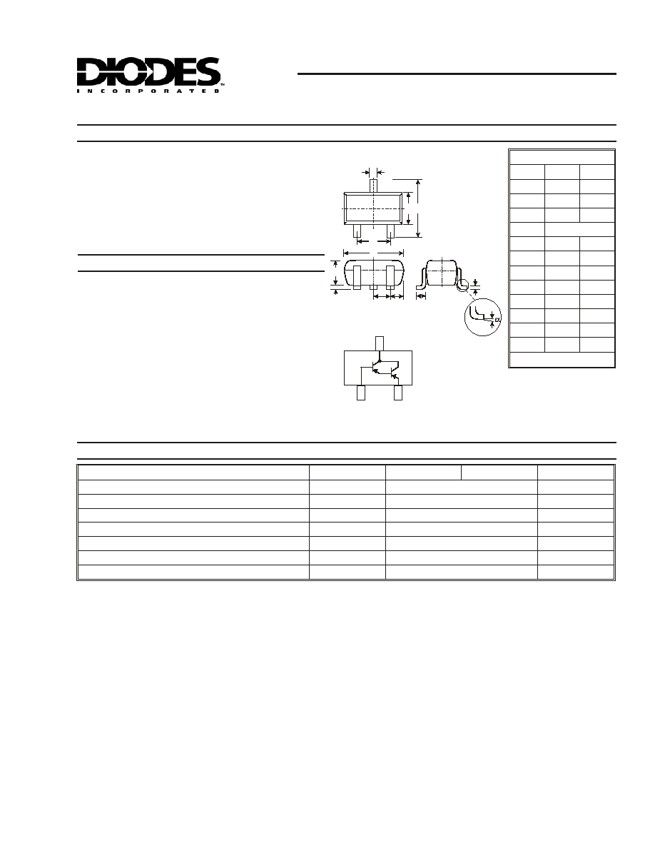
Mechanical Data
∑
Case: SOT-323, Molded Plastic
∑
Case Material - UL Flammability Rating 94V-0
∑
Moisture sensitivity: Level 1 per J-STD-020A
∑
Terminals: Solderable per MIL-STD-202,
Method 208
∑
Terminal Connections: See Diagram
∑
MMSTA63 Marking K2E, K3E (See Page 2)
∑
MMSTA64 Marking K3E (see Page 2)
∑
Ordering & Date Code Information: See Page 2
∑
Weight: 0.006 grams (approx.)
SOT-323
Dim
Min
Max
A
0.25
0.40
B
1.15
1.35
C
2.00
2.20
D
0.65 Nominal
E
0.30
0.40
G
1.20
1.40
H
1.80
2.20
J
0.0
0.10
K
0.90
1.00
L
0.25
0.40
M
0.10
0.18
a
0
∞
8
∞
All Dimensions in mm
Note:
1. Device mounted on FR-4 PCB, 1 inch x 0.85 inch x 0.062 inch; pad layout as shown on Diodes Inc. suggested pad layout
document AP02001, which can be found on our website at http://www.diodes.com/datasheets/ap02001.pdf.
C
E
B
DS30159 Rev. 3 - 2
2 of 2
MMSTA63/MMSTA64
www.diodes.com
Characteristic
Symbol
Min
Max
Unit
Test Condition
OFF CHARACTERISTICS (Note 2)
Collector-Emitter Breakdown Voltage
V
(BR)CEO
-30
æ
V
I
C
= -100
mA V
BE
= 0V
Collector Cutoff Current
I
CBO
æ
-100
nA
V
CB
= -30V, I
E
= 0
Emitter Cutoff Current
I
EBO
æ
-100
nA
V
EB
= -10V, I
C
= 0
ON CHARACTERISTICS (Note 2)
DC Current Gain
MMSTA63
MMSTA64
MMSTA63
MMSTA64
h
FE
5,000
10,000
10,000
20,000
æ
æ
I
C
= -10mA, V
CE
= -5.0V
I
C
= -10mA, V
CE
= -5.0V
I
C
= -100mA, V
CE
= -5.0V
I
C
= -100mA, V
CE
= -5.0V
Collector-Emitter Saturation Voltage
V
CE(SAT)
æ
-1.5
V
I
C
= -100mA, I
B
= -100
mA
Base- Emitter Saturation Voltage
V
BE(SAT)
æ
-2.0
V
I
C
= -100mA, V
CE
= -5.0V
SMALL SIGNAL CHARACTERISTICS
Current Gain-Bandwidth Product
f
T
125
æ
MHz
V
CE
= -5.0V, I
C
= -10mA,
f = 100MHz
Electrical Characteristics
@ T
A
= 25
∞C unless otherwise specified
Ordering Information
(Note 3)
Device
Packaging
Shipping
MMSTA63-7
SOT-323
3000/Tape & Reel
MMSTA647
SOT-323
3000/Tape & Reel
Notes:
2. Short duration test pulse used to minimize self-heating effect.
3. For Packaging Details, go to our website at http://www.diodes.com/datasheets/ap02007.pdf.
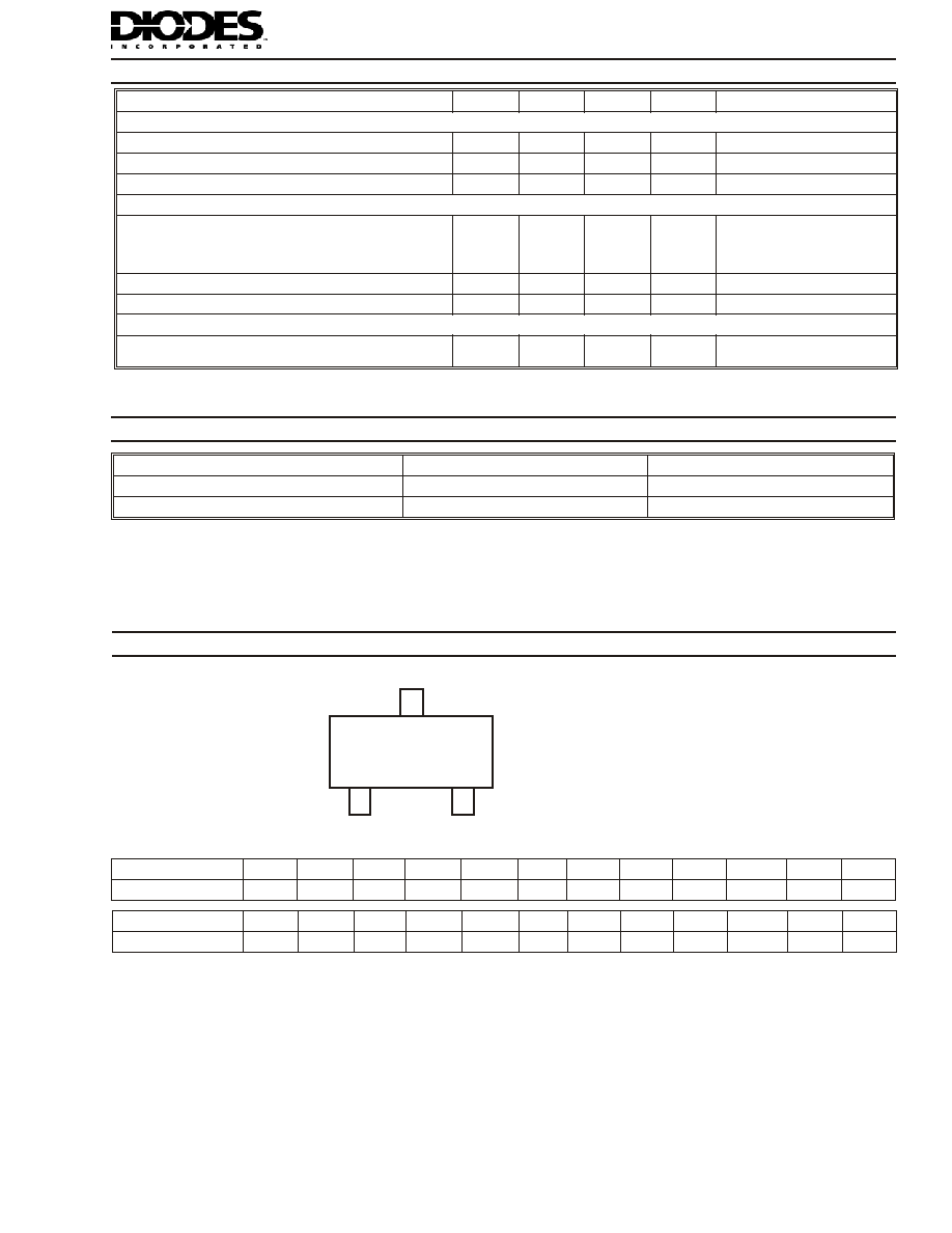
Marking Information
KxE
YM
KxE = Product Type Marking Code, e.g. K2E = MMSTA63
YM = Date Code Marking
Y = Year ex: N = 2002
M = Month ex: 9 = September
Date Code Key
Year
1998
1999
2000
2001
2002
2003
2004
2005
2006
2007
2008
2009
Code
J
K
L
M
N
P
R
S
T
U
V
W
Month
Jan
Feb
March
Apr
May
Jun
Jul
Aug
Sep
Oct
Nov
Dec
Code
1
2
3
4
5
6
7
8
9
O
N
D