DS19003 Rev. 11 - 2
1 of 3
SMCJ5.0(C)A - SMCJ170(C)A
SMCJ5.0(C)A - SMCJ170(C)A
1500W SURFACE MOUNT TRANSIENT VOLTAGE
SUPPRESSOR
∑
1500W Peak Pulse Power Dissipation
∑
5.0V - 170V Standoff Voltages
∑
Glass Passivated Die Construction
∑
Uni- and Bi-Directional Versions Available
∑
Excellent Clamping Capability
∑
Fast Response Time
∑
Plastic Case Material has UL Flammability
Classification Rating 94V-0
Features
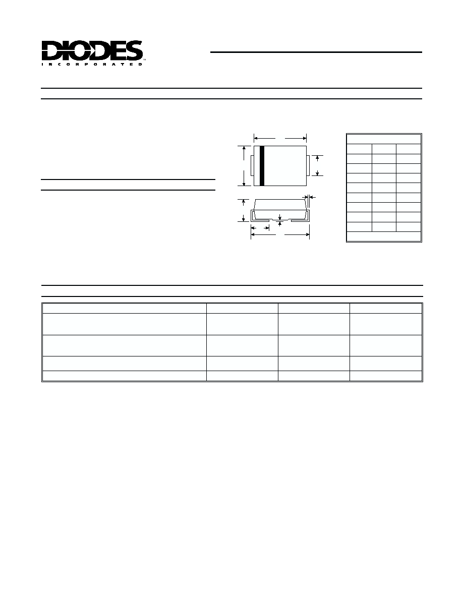
Mechanical Data
Maximum Ratings
@ T
A
= 25∞C unless otherwise specified
SMC
Dim
Min
Max
A
5.59
6.22
B
6.60
7.11
C
2.75
3.18
D
0.15
0.31
E
7.75
8.13
G
0.10
0.20
H
0.76
1.52
J
2.00
2.62
All Dimensions in mm
A
B
C
D
G
H
E
J
Notes:
1. Valid provided that terminals are kept at ambient temperature.
2. Measured with 8.3ms single half sine-wave. Duty cycle = 4 pulses per minute maximum.
3. Unidirectional units only.
∑
Case: SMC, Transfer Molded Epoxy
∑
Terminals: Solderable per MIL-STD-202,
Method 208
∑
Polarity Indicator: Cathode Band
(Note: Bi-directional devices have no polarity
indicator.)
∑
Marking: Date Code and Marking Code
See Page 3
∑
Weight: 0.21 grams (approx.)
Characteristic
Symbol
Value
Unit
Peak Pulse Power Dissipation
(Non repetitive current pulse derated above T
A
= 25∞C)
( Note 1)
P
PK
1500
W
Peak Forward Surge Current, 8.3ms Single Half Sine
Wave Superimposed on Rated Load (JEDEC Method)
(Notes 1, 2, & 3)
I
FSM
200
A
Instantaneous Forward Voltage @I
PP
= 35A
(Notes 1, 2, & 3)
V
F
3.5
V
Operating and Storage Temperature Range
T
j
, T
STG
-55 to +150
∞C
DS19003 Rev. 11 - 2
3 of 3
SMCJ5.0(C)A - SMCJ170(C)A
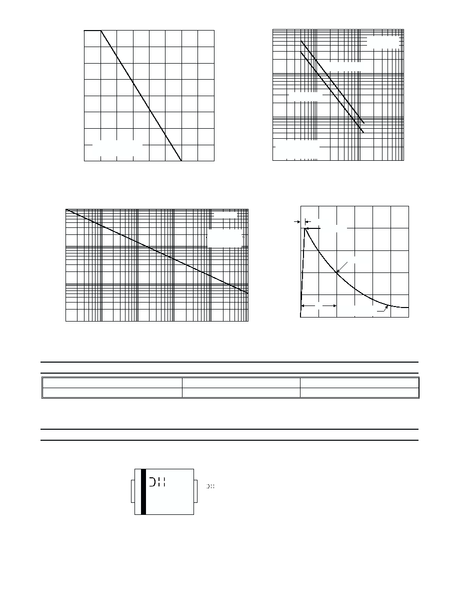
1
10
100
1000
10
100
1000
10,000
V
, REVERSE STANDOFF VOLTAGE (V)
Fig. 2 Typical Junction Capacitance
RWM
C
,
CAP
ACIT
ANCE
(pF)
j
T = 25 C
f = 1.0 MHz
j
∞
V = 50mV p-p
sig
Measured at
zero bias
Uni-directional
Bi-directional
0.1
1.0
t PULSE WIDTH ( s)
Fig. 3 Pulse Rating Curve
p
m
0.1
10
100
1.0
10
1000
10000
T = 25 C
j
∞
P
,
PEAK
PULSE
POWER
(kW)
d
100
Non Repetitive
Pulse Waveform
Shown in Fig. 4
0
1
2
3
100
50
0
I
,
PEAK
PULSE
CURRENT
(%I
)
Pp
p
t = 10 s
r
m
Peak Value I
pp
Half Value I /2
pp
10 X 1000 Waveform
as defined by R.E.A.
t
p
t, TIME (ms)
Fig. 4 Pulse Waveform
10 X 1000 Waveform
as defined by REA
0
25
50
75 100 125 150 175 200
100
75
50
25
0
T , AMBIENT TEMPERATURE ( C)
Fig. 1 Pulse Derating Curve
A
∞
PEAK
PULSE
DERA
TING
IN
%
O
F
PEAK
POWER
OR
CURRENT
XXX = Product type marking code (See Page 2)
= Manufacturers' code marking
YWW = Date code marking
Y = Last digit of year ex: 2 for 2002
WW = Week code 01 to 52
YWW
XXX
Marking Information
Notes:
4. For Packaging Details, go to our website at http://www.diodes.com/datasheets/ap02007.pdf.
Device
Packaging
Shipping
SMCJXXX(C)A-13
SMC
5000/Tape & Reel
Ordering Information
(Note 4)