
DIONICS, INC.
Phone: (516) 997-7474
65 Rushmore Street Fax: (516) 997-7479
Westbury, NY 11590 Website: www.dionics-usa.com
LEVEL-SHIFTED GAS DISCHARGE DISPLAY DIGIT DRIVERS
DI-507B DI-512B
General Description:
The DIONICS DI-507B and DI-512B series circuits are
designed for interfacing between MOS or TTL circuitry and
gas discharge display panels. Each section of these devices is
made up of a switched constant current level shifter-capable of
high voltage operation and a PNP-NPN driver transistor pair.
The constant current operation of the level shifter stage results
in low power dissipation. Input circuitry is suitable for open
drain PMOS, CMOS, open-collector or standard TTL.
Features:
¸
125V Level Shift Capability
¸
MOS and TTL Compatibility
¸
6- and 8-line Versions
¸
Low Power Dissipation
¸
Reliable Dielectric Isolation Process
¸
Pin For Pin Replacement for
Sprague UDN-6164A, UDN-6184A
¸
Functional Replacement For SIGNETICS 585 Series
Package Layout:
DI-507B
DI-512B
0.185
0.070
0.250
0.025
DIONICS INC
DI-507B
0.800
0.020
5
In
4
In
3
1
15
In
2
GND
16
V +
14
NC
13
Out
12
Out
11
Out
10
Out
9
In
Out
8
NC
7
Out
In
6
In
0.250
0.900
0.185
0.025
0.020
0.070
DIONICS INC
DI-512B
17
8
1
Out
2
4
V +
9
Out
GND
14
In
In
In
In
In
Out
11
Out
6
Out
In
Out
16
In
Out
15
12
In
13
3
5
18
7
10
Out
01/2002
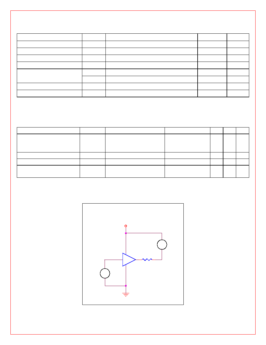
Circuit Schematic
(Each Section)
V+
Output
Input
Absolute Maximum Rating (Ta = 25
0
C)
Characteristic
Symbol
Notes
Limits
Units
Supply Voltage
V +
Measured With Respect to GND
125
V
Input Voltage
V
in
Measured With Respect to GND
35
V
Output Voltage
V
out
Measured With Respect to V + Terminal
90
V
Output Current
I
out
40
mA
Power Dissipation DI-512B
P
D
Derate at 8 mW/
0
C Above 25
0
C Ambient
800
mW
DI-507B
P
D
Derate at 6 mW/
0
C Above 25
0
C Ambient
600
mW
Storage Temperature
T
s
-55 to +125
0
C
Operating Temperature
T
o
0 to +70
0
C
Electrical Characteristics (Ta = 25
0
C)
Parameter
Symbol
Notes
Conditions
Typ. Max. Units
Output Saturation
Voltage
V
out
(SAT)
V + = 100V; Measured
With Respect to V+
Terminal
I
o
= 25mA;
V
i
= 2.4V
3
10
V
Output Leakage Current
I
out
(OFF)
V + = 180V
V
o
= 90V; V
i
= 0.4V 0.1 10 µA
Input Current
I
in
(ON)
V
i
= 2.4V
340 400 µA
Supply Current
I+
One Input at 2.4V, Others
at 0.4V
V+ = 100V;
V
i
= 2.4 V; I
o
= 0
0.5 1.5 mA
+ 100V
-
GND
V in
Simplified Test Circuit
+
-
80 V
+
V +
R load
4 K