
MECHANICAL DATA
FEATURES
Data Sheet No. SEDR-3000-1B
MECHANICAL SPECIFICATION
Case: TO-247(TO-3P) molded plastic
(U/L Flammability Rating 94V-0)
Terminals: Rectangular pins w/ standoff
Solderability: Per MIL-STD 202 Method 208 guaranteed
Polarity: Diodes depicted on product
Mounting Position: Any
Weight: 0.2 Ounces (5.55 Grams)
D9
Average Forward Rectified Current @ Tc = 100 C
o
MAXIMUM RATINGS & ELECTRICAL CHARACTERISTICS
Ratings at 25 ∞C ambient temperature unless otherwise specified.
Single phase, half wave, 60Hz, resistive or inductive load.
For capacitive loads, derate current by 20%.
PARAMETER (TEST CONDITIONS)
Maximum DC Blocking Voltage
Maximum Peak Recurrent Reverse Voltage
Maximum RMS Voltage
Series Number
I
O
V
RMS
V
RRM
V
RM
SYMBOL
RATINGS
UNITS
VOLTS
30
UFR
UFR
UFR
UFR
UFR
100
200
300
400
100
200
300
400
70
140
210
280
500
350
500
(1) Measured at 1 MHz and an applied reverse voltage of 4 volts.
Peak Forward Surge Current ( 8.3mS single half sine wave
superimposed on rated load)
Maximum Forward Voltage (per diode) at 15 Amps DC
VOLTS
AMPS
V
FM
I
FSM
250
200
1.0
Typical Thermal Resistance, Junction to Case
Junction Operating and Storage Temperature Range
Maximum Average DC Reverse Current
At Rated DC Blocking Voltage
I
RM
R
JC
T
J,
T
STG
∞C/W
∞C
µ
A
Typical Junction Capacitance (Note 1)
C
J
pF
@ T = 25 C
C
o
@ T = 100 C
C
o
10
500
2
150
-65 to +150
4.97fsedr10
NOTES:
Maximum Reverse Recovery Time (I =15.0A, di/dt=50A/ S,T =25 C)
F
J
µ
o
T
RR
nSec
1.25
50
60
3001C
3002C
3003C
3004C
3005C
Glass Passivated for high reliability/temperature performance
Low switching noise
Low forward voltage drop
Low thermal resistance
High switching capability
High surge capability
Tel.: (310) 767-1052
Fax: (310) 767-7958
DIOTEC ELECTRONICS CORP
Gardena, CA 90248
U.S.A
18020 Hobart Blvd., Unit B
0.087
0.075
0.045
0.022
0.079
0.116
0.776
0.209
0.146
A
A1
A2
B
B1
B2
B3
B4
C
D
D1
L
L1
Sym
in
mm
0.19
4.82
2.21
1.9
1.14
0.56
2.01
2.95
0.602 15.29
19.7
5.31
0.559 14.2
3.71
0.102
0.085
0.055
0.032
0.094
0.215
0.799
0.224
0.189
in
mm
0.205
5.2
2.6
2.16
1.4
0.81
2.39
5.46
0.625
15.88
20.3
5.69
0.582
14.8
4.8
0.13
P
RO 0.209
5.3
3.3
0.145
0.224
5.7
3.7
Minimum
Maximum
0.126
3.2
A2
L
A1
B
B1
B2*
B3
B4
B4
D
L1
RO
A
D1
C
*Applies to Pins 1 and 3
1
2
2
3
DT 7D
UFR3002C
DT 7D
UFR3002C
TO-247AB (TO-3PAB)
SERIES UFR3001C - UFR3005C
ACTUAL SIZE OF TO-247AB
(TO-3PAB) PACKAGE
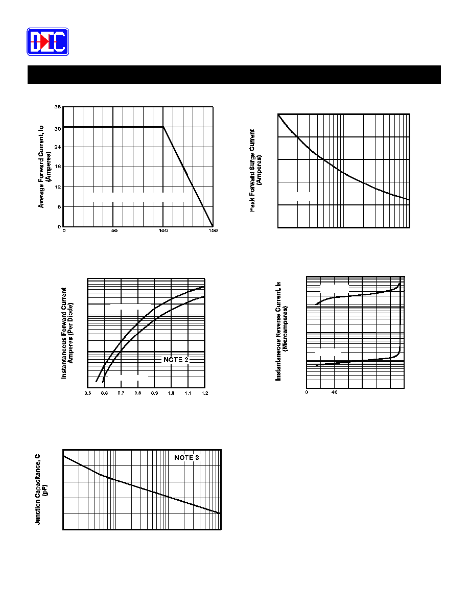
RATING & CHARACTERISTIC CURVES FOR SERIES UFR3001C - UFR3005C
Data Sheet No. SEDR-3000-2B
FIGURE 4. TYPICAL REVERSE CHARACTERISTICS
FIGURE 3. TYPICAL FORWARD CHARACTERISTICS
Instantaneous Forward Voltage (Volts)
10
1.0
100
0.1
Percent of Rated Peak Reverse Voltage
0.001
0.01
0.1
1.0
10
30 AMP ULTRAFAST RECOVERY DIODES
4.97bsedr30
100
120
140
NOTES
(1) JEDEC Method, 8.3 mSec. Single Half Sine Wave
(2) T = 25 C, Pulse Width = 300 Sec, 2.0% Duty Cycle
(3) T = 25 C, f = 1 MHz, V
= 50 mV P-P
J
C
SIG
o
o
µ
D10
T = 100 C
C
o
T = 25 C
C
o
20
60
80
FIGURE 5. TYPICAL JUNCTION CAPACITANCE
Reverse Voltage, (Volts)
1
10
100
180
120
60
0
240
300
0.1
FIGURE 1. FORWARD CURRENT DERATING CURVE
Case Temperature, C
o
Resistive and Inductive Loads
FIGURE 2. MAXIMUM NON-REPETITIVE SURGE CURRENT
Number of Cycles at 60 Hz
1
10
100
250
200
150
100
50
0
NOTE 1
UFR3003C-3005C
UFR3001C-3002C
Tel.: (310) 767-1052
Fax: (310) 767-7958
DIOTEC ELECTRONICS CORP.
Gardena, CA 90248
U.S.A
18020 Hobart Blvd., Unit B