e
1
PTF 10009
85 Watts, 1.0 GHz
GOLDMOS
TM
Field Effect Transistor
10009
1234569744
0
10
20
30
40
50
60
70
80
90
100
0.0
1.0
2.0
3.0
4.0
5.0
Input Power (Watts)
Ou
t
p
u
t
P
o
wer
0
8
16
24
32
40
48
56
64
72
80
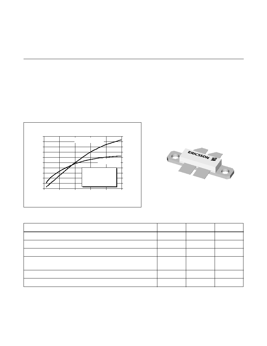
Efficiency
V
DS
= 28 V
I
DQ
= 600 mA Total
f = 960 MHz
Typical Output Power and Efficiency vs. Input Power
Efficiency (%)
Output Power (W)
Package 20230
�
Performance at 960 MHz, 28 Volts
- Output Power = 85 Watts
- Power Gain = 13.0 dB Typ
- Efficiency = 50% Typ
�
Full Gold Metallization
�
Silicon Nitride Passivated
�
Excellent Thermal Stability
�
100% lot traceability
Description
The PTF 10009 is an 85 Watt LDMOS FET intended for large signal
amplifier applications to 1.0 GHz. It operates at 50% efficiency and
13.0 dB of gain. Nitride surface passivation and full gold metallization
are used to ensure excellent device lifetime and reliability.
Maximum Ratings
Parameter
Symbol
Value
Unit
Drain-Source Voltage
(1)
V
DSS
65
Vdc
Gate-Source Voltage
(1)
V
GS
�20
Vdc
Operating Junction Temperature
T
J
200
�C
Total Device Dissipation
P
D
270
Watts
Above 25�C derate by
1.54
W/�C
Storage Temperature Range
T
STG
-65 to 150
�C
Thermal Resistance (T
CASE
= 70�C)
R
q
JC
0.65
�C/W
(1)
per side
All published data at T
CASE
= 25�C unless otherwise indicated.
2
PTF 10009
e
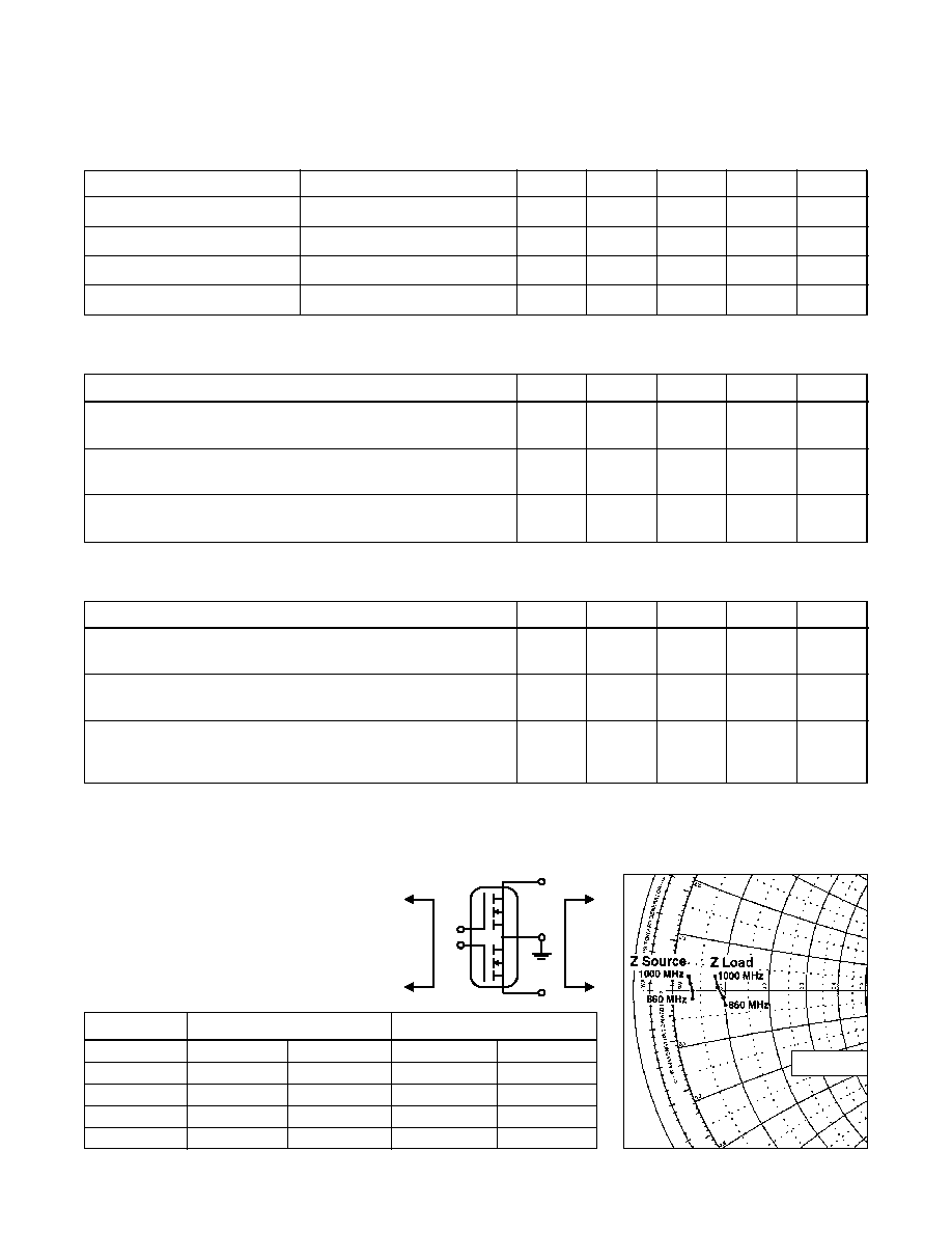
Frequency
Z Source
W
Z Load
W
MHz
R
jX
R
jX
860
1.76
-0.78
5.00
-1.50
900
1.80
-0.05
4.80
-0.78
960
1.58
0.69
4.24
0.36
1000
1.39
1.35
3.95
1.41
Electrical Characteristics
(100% Tested--characteristics, conditions and limits shown per side)
Characteristic
(per side)
Conditions
Symbol
Min
Typ
Max
Units
Drain-Source Breakdown Voltage V
GS
= 0 V, I
D
= 25 mA
V
(BR)DSS
65
--
--
Volts
Drain-Source Leakage Current
V
DS
= 28 V, V
GS
= 0 V
I
DSS
--
--
1.0
mA
Gate Threshold Voltage
V
DS
= 10 V, I
D
= 75 mA
V
GS(th)
3.0
--
5.0
Volts
Forward Transconductance
V
DS
= 10 V, I
D
= 3 A
g
fs
--
2.8
--
Siemens
Dynamic Characteristics
Characteristic
(per side)
Symbol
Min
Typ
Max
Units
Input Capacitance
(V
DS
= 28 V, V
GS
= 0 V, f = 1 MHz)
C
iss
--
90
--
pF
Output Capacitance
(V
DS
= 28 V, V
GS
= 0 V, f = 1 MHz)
C
oss
--
36
--
pF
Reverse Transfer Capacitance
(V
DS
= 28 V, V
GS
= 0 V, f = 1 MHz)
C
rss
--
1.9
--
pF
RF Specifications
(100% Tested)
Characteristic
Symbol
Min
Typ
Max
Units
Gain
(V
DD
= 28 V, Pout = 85 W, I
DQ
= 600 mA, f = 960 MHz)
G
ps
12.0
13.0
--
dB
Drain Efficiency
(V
DD
= 28 V, Pout = 85 W, I
DQ
= 600 mA, f = 960 MHz)
h
47
50
--
%
Load Mismatch Tolerance
(V
DD
= 28 V, Pout = 85 W, I
DQ
= 600 mA, f = 960 MHz--
Y
--
--
5:1
--
all phase angles at frequency of test)
Impedance Data
(data shown for fixed-tuned broadband circuit)
(V
DD
= 28 V, Pout = 85 W, I
DQ
= 600 mA)
Z Source
Z Load
G
D
G
S
D
Z
0
= 50
W
3
PTF 10009
e
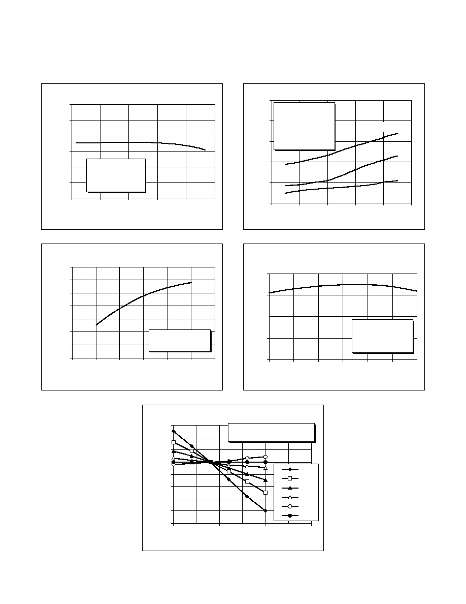
Typical Performance
Gain vs. Power Output
5.0
7.5
10.0
12.5
15.0
17.5
20.0
0
20
40
60
80
100
Output Power (Watts)
G
a
in (dB)
V
DS
= 28 V
I
DQ
= 600mA Total
f = 960 MHz
Intermodulation Distortion vs. Output Power
-60
-50
-40
-30
-20
-10
0
20
40
60
80
100
Output Power (Watts-PEP)
IM
D (dBc
)
V
DS
= 28V
I
DQ
= 600 mA Total
f
1
= 960.0 MHz
f
2
= 960.1 MHz
3rd Order
5th
7th
Output Power vs. Drain-Source Voltage
65
70
75
80
85
90
95
100
22
24
26
28
30
32
34
Drain-Source Voltage (Volts)
Output Power (Watts)
I
DQ
= 600 mA Total
f = 960 MHz
Gain vs. Frequency
(as measured in a broadband circuit)
10
11
12
13
14
900
910
920
930
940
950
960
Frequency (MHz)
G
a
in (dB)
V
DS
= 28 V
I
DQ
= 600 mA Total
Pout = 85 W
Bias Voltage vs. Temperature
0.95
0.96
0.97
0.98
0.99
1.00
1.01
1.02
1.03
-20
30
80
130
Temp. (�C)
Bias Voltage (V)
0.43
1.25
2.08
2.9
3.71
4.53
Voltage normalized to 1.0 V
Series show current (A)

4
PTF 10009
e
Typical Scattering Parameters
(V
DS
= 28 V, I
D
= 1.0 A per side)
f
S11
S21
S12
S22
(MHz)
Mag
Ang
Mag
Ang
Mag
Ang
Mag
Ang
40
0.883
-153
33.0
93
0.014
3
0.527
-143
60
0.878
-160
21.8
85
0.013
1
0.533
-148
80
0.876
-163
16.1
80
0.012
-6
0.553
-150
100
0.884
-164
12.8
76
0.012
-13
0.574
-148
150
0.904
-165
8.21
65
0.011
-18
0.638
-148
200
0.915
-165
5.67
58
0.010
-23
0.694
-149
250
0.934
-164
4.36
51
0.010
-31
0.769
-148
300
0.947
-164
3.41
45
0.010
-31
0.792
-149
350
0.962
-163
2.78
41
0.008
-28
0.837
-150
400
0.975
-163
2.30
36
0.008
-33
0.873
-151
450
0.974
-163
1.90
33
0.006
-36
0.874
-151
500
0.977
-163
1.65
30
0.006
-52
0.912
-152
550
0.979
-164
1.44
27
0.005
-46
0.916
-154
600
0.985
-164
1.28
26
0.004
-53
0.925
-154
650
0.981
-165
1.14
22
0.003
-27
0.933
-156
700
0.980
-166
1.01
21
0.004
-18
0.933
-157
750
0.975
-167
0.924
19
0.003
-13
0.936
-158
800
0.973
-168
0.809
16
0.001
14
0.946
-160
850
0.972
-170
0.749
14
0.003
-1
0.939
-160
900
0.969
-171
0.656
12
0.003
30
0.946
-162
950
0.966
-173
0.609
14
0.002
53
0.948
-164
1000
0.969
-174
0.564
8
0.003
59
0.945
-164
1050
0.969
-176
0.526
3
0.004
56
0.949
-167
1100
0.970
-177
0.450
6
0.004
69
0.955
-167
1150
0.970
-178
0.405
1
0.005
57
0.953
-168
1200
0.970
-179
0.383
4
0.005
65
0.952
-169
1250
0.971
180
0.351
-5
0.005
56
0.959
-170
1300
0.971
179
0.330
-5
0.005
61
0.957
-170
1350
0.973
179
0.308
-5
0.005
52
0.963
-171
1400
0.973
179
0.255
-3
0.006
59
0.965
-171
1450
0.972
179
0.219
5
0.006
58
0.965
-171
1500
0.965
179
0.210
-8
0.006
62
0.957
-172
5
PTF 10009
e
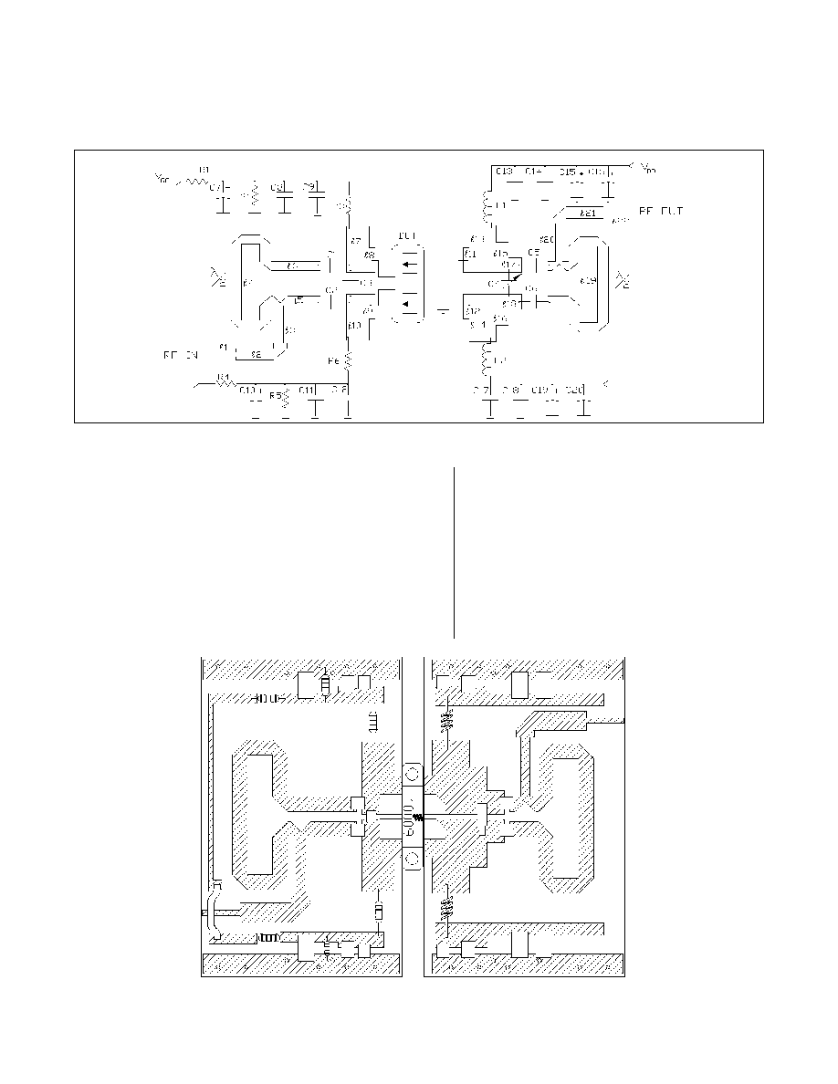
Parts Layout (not to scale)
Test Circuit
Schematic for f = 960 MHz
DUT
10009
C1-2, C5-6, C9, C12-13, C17 33 pF, Capacitor ATC 100 B
C3
11 pF, Capacitor ATC 100 B
C4
6.0 pF, Variable Capacitor, JMC 5701
C7, C10
10
m
F, +10 V Electrolytic Capacitor
C8, C11, C14, C18
0.01
m
F, Capacitor ATC 100 B
C15, C16, C19, C20
10
m
F, +30 V Electrolytic Capacitor
L1. L2
4 Turn, #20 AWG, .120" I.D.
R1, R2, R4, R5
1.0 K,
W
Resistor
R3, R6
5.1 K, 1/4
W
Resistor
l
1,
l
22
50
W
, .030
l
l
2,
l
21
20
W
, .080
l
l
3,
l
20
32
W
, .191
l
l
4,
l
19
25
W
, .500
l
l
5,
l
6
25
W
, .091
l
l
7,
l
10
7
W
, .056
l
l
8,
l
9
13.0
W
, .017
l
l
11,
l
12
13.0
W
, .017
l
l
13,
l
14
7.0
W
, .064
l
l
15,
l
16
10.0
W
, .029
l
l
17,
l
18
19.0
W
, .028
l
Circuit Board
.031" Dielectric Thickness,
e
r
= 4.0,
AlliedSignal, G200, 2 oz. copper