 | –≠–ª–µ–∫—Ç—Ä–æ–Ω–Ω—ã–π –∫–æ–º–ø–æ–Ω–µ–Ω—Ç: 225A833 | –°–∫–∞—á–∞—Ç—å:  PDF PDF  ZIP ZIP |
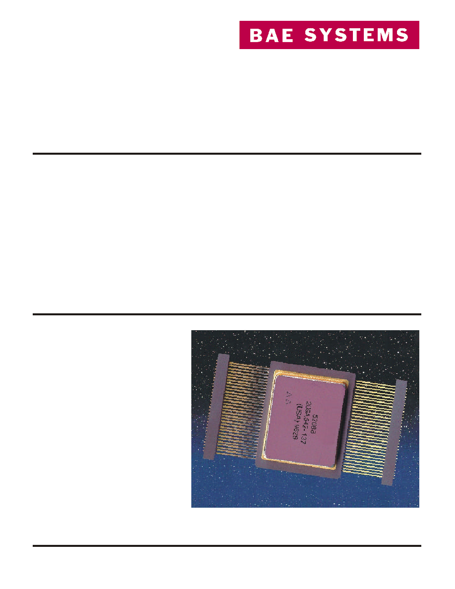
128K x 32
Radiation Hardened
Static RAM MCM≠ 5 V
225A833
BAE SYSTEMS ∑ 9300 Wellington Road ∑ Manassas, Virginia 20110-4122
Product Description
Radiation
∑ Fabricated with Bulk CMOS 0.5 µm Process
∑ Total Dose Hardness through 1x10
6
rad(Si)
∑ Neutron Hardness through 1x10
14
N/cm
2
∑ Dynamic and Static Transient Upset Hardness
through 1x10
9
rad(Si)/s
∑ Soft Error Rate of < 1x10
-11
Upsets/Bit-Day
∑ Latchup Free
Features
Other
∑ Read/Write Cycle Times
25 ns (-55 ∞C to 125∞C)
∑ SMD Number Pending
∑ Asynchronous Operation
∑ CMOS or TTL Compatible I/O
∑ Single 5 V ± 10% Power Supply
∑ Low Operating Power
∑ Packaging Options
∑ 64-Lead Dual Flat Pack (1.000" x 0.900")
General Description
The 128K x 32 radiation hardened static
RAM is composed of four 128K x 8 SRAM
memory die assembled in a single, double-
sided ceramic substrate. Each die is a high
performance 131,072 word x 8-bit static
random access memory with industry-
standard functionality. It is fabricated with
BAE SYSTEMS' radiation hardened
technology and is designed for use in
systems operating in radiation
environments. The RAM operates over the
full military temperature range and requires
a single 5 V ± 10% power supply. The RAM
is available with CMOS compatible I/O.
Power consumption is typically less than 80
mW/MHz in operation, and less than 40 mW
in the low power disabled mode. The RAM
read operation is fully asynchronous, with an
associated typical access time of 19
nanoseconds.
BAE SYSTEMS' enhanced bulk CMOS
technology is radiation hardened through
the use of advanced and proprietary design,
layout, and process hardening techniques.
2
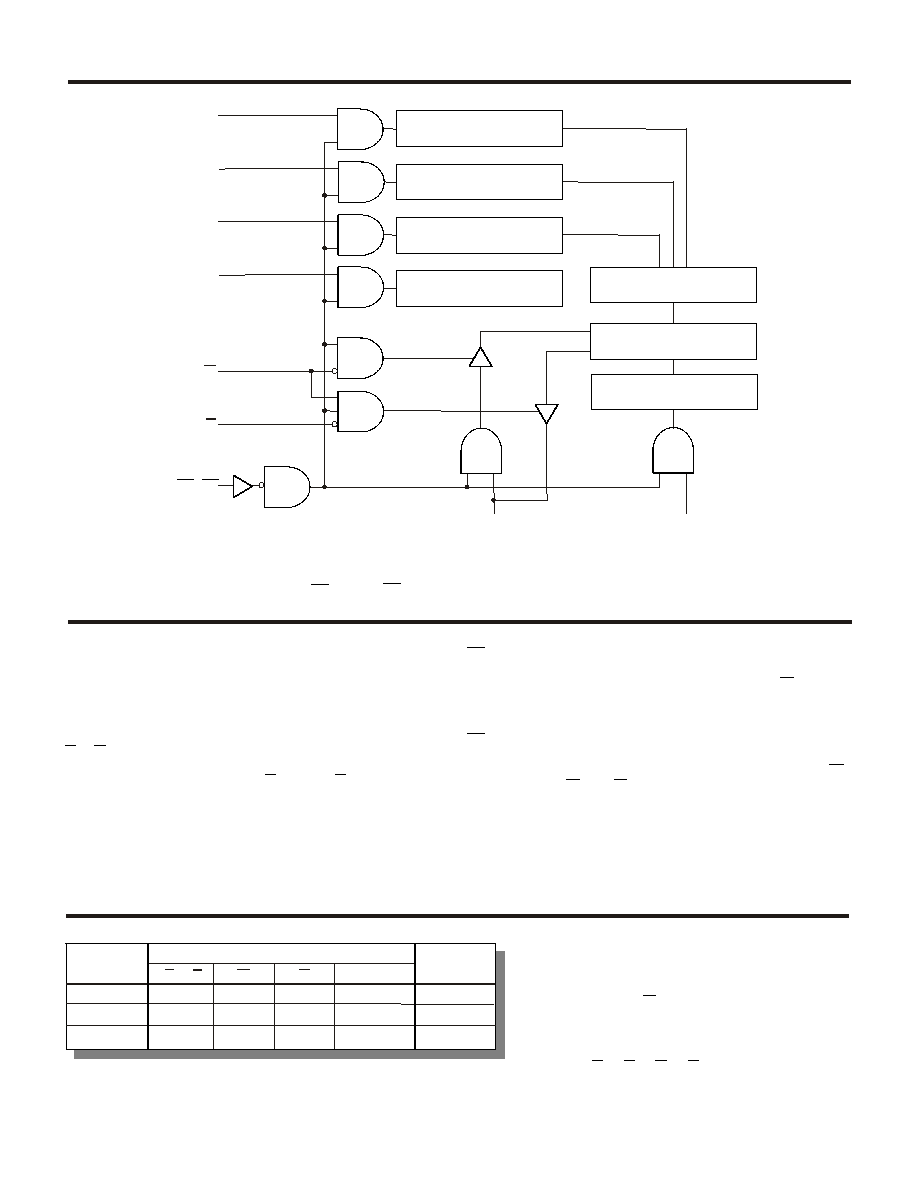
Functional Diagram
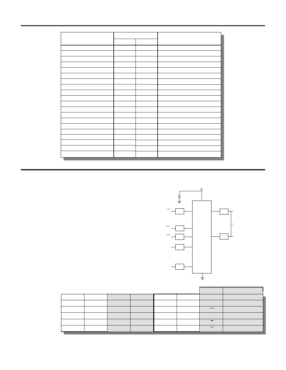
Signal Definitions
A: 0-16
DQ: 0-31
S1 - S4
≠ Address input pins that select a particular
eight-bit word within the memory array.
≠ Bi-directional data pins that serve as data
outputs during a read operation and as
data inputs during a write operation.
≠ Negative chip select, when at a low level,
allows normal read or write operation.
When at a high level, S1 through S4 forces
the SRAM to a precharge condition, holds
the data output drivers in a high
impedance state and disables the data
input buffers only. If this signal is not used,
it must be connected to GND.
≠ Negative write enable, when at a low level, activates a
write operation and holds the data output drivers in a
high impedance state. When at a high level, W allows
normal read operation.
≠ Negative output enable, when at a high level holds the
data output drivers in a high impedance state. When at
a low level, the data output driver state is defined by S1
through S4, and W. If this signal is not used it must be
connected to GND.
W
G
Notes:
1) V
IN
for don't care (X) inputs = V
IL
or V
IH
.
2) When G = high, I/O is high-Z.
3) To dissipate the minimum amount of
standby power when in standby mode:
S1 = S2 = S3 = S4 = V
DD
. All other input
levels may float.
Truth Table
A0
A1 - A2
A3
A9 - A16
W
G
S1 - S4
DQ0-DQ31
A4-A8
Top/Bottom Decoder
Block Address Decoder
L/R Side/Block
Row Address Decoder
(((256 x 32) x 2 x 4) x 8 x 2) x 4
Memory Cell Array
32 Bit Word Input/Output
Column Address Decoder
Note:
1) All package leads are common with top and bottom SRAM devices
except for S1 through S4.
Mode
Inputs
(1),(2)
S1 - S4
Low
Low
High
W
Low
High
X
G
X
Low
X
I/O
Data-In
Data-Out
High-Z
Power
Active
Active
Standby
Write
Read
Standby
(3)
3
Notes:
1)All voltages referenced to GND.
Power shall be applied to the device only in the following
sequences to prevent damage due to excessive currents:
∑ Power-Up Sequence: GND, V
DD
, Inputs
∑ Power-Down Sequence: Inputs, V
DD
, GND
Absolute Maximum Ratings
Recommended Operating Conditions
Power Sequencing
Note:
Minimum
+4.5
0.0
-55
-0.3
+3.5
Units
Volt
Volt
Celsius
Volt
Volt
Supply Voltage
Parameters
(1)
Supply Voltage Reference
Case Temperature
Input Logic "Low"
Input Logic "High"
Symbol
V
DD
GND
T
C
V
IL
V
IH
Maximum
+5.5
0.0
+125
+1.5
V
DD
1) Stresses above the absolute maximum rating may cause permanent
damage to the device. Extended operation at the maximum levels may
degrade performance and affect reliability. All voltages are with
reference to the module ground leads.
2) Maximum applied voltage shall not exceed +7.0 V.
3) Guaranteed by design; not tested.
4) Class as defined in MIL-STD-883, Method 3015.
5) Typical power dissipation = 2.0 W.
6) It is recommended that the part be thermally bonded to the board.
Minimum
-70∞C
-55∞C
-0.5 V
-0.5 V
-0.5 V
(Class II)
Storage Temperature Range (Ambient)
Applied Conditions
(1)
Operating Temperature Range (T
case
)
Positive Supply Voltage
Input Voltage
(2)
Output Voltage
(2)
Power Dissipation
(3)
Lead Temperature (Soldering 5 sec)
Electrostatic Discharge Sensitivity
(4)
Maximum
+150∞C
+125∞C
+7.0 V
V
DD
+ 0.5 V
4.0 W
(5)
3∞C/W
V
DD
+ 0.5 V
Thermal Resistance, Junction-to-Case (
JC
)
(6)
+230∞C
4
1) Typical operating conditions: Vdd
5.0 V; TA = 25∞C, pre-radiation.
-55∞C
T
case
+125∞C; 4.5 V
V
DD
5.5 V; unless otherwise specified.
2) By Design / Verified by Characterization
3) The worst case timing sequence of t
WLQZ
+ t
DVWH
+ t
WHWL
= t
AVAV
(write
cycle time)
300 ± 10%
2.8V
50 pF + 10%
Output Load Circuit
DC Electrical Characteristics
Notes:
Symbol
Test Conditions
(1)
Device
Type
Limits
Minimum
Maximum
Units
I
DD1
V
OH
F = F
MAX
= 1/t
AVAV(min)
No Output Load
V
DD
= 2.5 V
0 V
V
IN
5.5 V
I
OH
= -200 µA
I
OH
= -4 mA
I
OL
= 200 µA
I
OL
= 8 mA
All
All
All
All
All
All
All
All
All
All
All
720
8.0
8.0
4.0
4.0
-10
-20
0.4
V
DD
- 0.5 V
0.05
1.5
20
40
50
40
mA
mA
mA
mA
V
µA
µA
pF
pF
V
V
Test
Supply Current
(Cycling Selected)
Supply Current
(Cycling De-Selected)
Supply Current
(Standby)
Data Retention Current
Low Level Input Voltage
Input Leakage
Output Leakage
C
in
C
out
High Level Output Voltage
Low Level Output Voltage
I
DD2
I
DD3
I
DR
V
OL
All
3.5
V
High Level Input Voltage
V
IH
V
IL
I
ILK
I
OLK
S1 = S2 = S3 = S4 = V
DD
F = F
MAX
= 1/t
AVAV(min)
F = 0 MHz
S1 = S2 = S3 = S4 = V
DD
0 V
V
OUT
5.5 V
All
2.5
V
Data Retention Voltage
V
DR
(3)
V
DD
= V
DR
Group A
Sub-Groups
1, 2, 3
1, 2, 3
1, 2, 3
1, 2, 3
1, 2, 3
1, 2, 3
1, 2, 3
1, 2, 3
1, 2, 3
1, 2, 3
1, 2, 3
CMOS
TTL
CMOS
TTL
(2)
(2)
2.0
0.8
Note:
1)Test conditions: input switching levels V
IL
/V
IH
= 0.5 V/V
DD
-0.5 V (CMOS), input rise and fall times < 5 ns,
input and output timing reference levels shown in the Tester AC Timing Characteristics table, capacitive output
loading C
L
= 50 pF. For C
L
> 50 pF, derate access times by 0.02 ns/pF (typical). -55 ∞C
T
case
+125∞C;
4.5 V
V
DD
5.5 V; unless otherwise specified.
5
Read Cycle AC Timing Characteristics
(1)
Read Cycle Timing Diagram
Valid Address
Valid Data
High Impedance
Address
S1 - S4
G
Data
Out
t
AVAV
t
AVQV
t
SLQV
t
SLQX
t
GLQV
t
GLQX
t
AXQX
t
SHQZ
t
GHQZ
Limits
Units
ns
ns
ns
ns
ns
ns
ns
ns
ns
Test
Read Cycle Time
Chip Select to Output Active
Output Enable to Output Active
Address Access Time
Chip Select Access Time
Output Hold After Address Change
Chip Select to Output Disable
Output Enable to Output Disable
Output Enable Access Time
Minimum or
Maximum
Minimum
Minimum
Minimum
Maximum
Maximum
Minimum
Maximum
Maximum
Maximum
0
0
0
12
12
Symbol
t
AVAV
t
AVQV
t
SLQV
t
SLQX
t
SHQZ
t
AXQX
t
GLQV
t
GLQX
t
GHQZ
Device Type
30
X2X
X3X
25
30
X2X
X3X
25
30
X2X
X3X
25
12
X2X
X3X
10
All
All
All
All
All
1) Test conditions: input switching levels V
IL
/V
IH
= 0.5 V/V
DD
- 0.5 V (CMOS), input rise and fall times < 5 ns,
input and output timing reference levels shown in the Tester AC Timing Characteristics table, capacitive
output loading = 50 pF. -55∞C
T
case
+125∞C; 4.5 V
V
DD
5.5 V; unless otherwise specified.
2) Cycle time per individual die.
6
Write Cycle AC Timing Characteristics
(1)
Note:
Write Cycle Timing Diagram
t
AVAV
Valid Address
Valid Data
High Impedance
High Impedance
High Impedance
High Impedance
Address
t
AVWH
t
SLWH
t
WLWH
t
AVWL
t
WLQZ
t
WHQX
t
WHDX
t
WHWL
t
DVWH
S1 - S4
W
Data
Out
Data
In
t
WHAX
Units
ns
ns
ns
ns
ns
ns
ns
ns
ns
Test
Write Cycle Time
Chip Select to End of Write
Address Setup to End of Write
Address Hold After End of Write
Write Disable Pulse Width
Write Pulse Width
Data Setup to End of Write
Address Setup to Start of Write
Data Hold After End of Write
Write Enable to Output Disable
Output Active After End of Write
Minimum or
Maximum
Minimum
Minimum
Minimum
Minimum
Minimum
Minimum
Minimum
Minimum
Minimum
Maximum
Minimum
Symbol
t
AVAV
2
t
WLWH
t
SLWH
t
DVWH
t
AVWH
t
WHDX
t
AVWL
t
WHAX
t
WLQZ
t
WHQX
t
WHWL
Limits
Device Type
All
All
All
All
All
5
0
0
12
6
X2X
X3X
30
25
X2X
X3X
24
19
X2X
X3X
24
19
X2X
X3X
24
19
ns
X2X
X3X
24
19
ns
X2X
X3X
0
1

Write Cycle
The write operation is synchronous with respect to the
address bits, and control is governed by write enable (W)
and chip select (S1-S4) edge transitions (refer to Write
Cycle Timing diagrams). To perform a write operation,
both W and S1-S4 must be low. Consecutive write cycles
can be performed with W or S1-S4 held continuously low.
At least one of the control signals must transition to the
opposite state between consecutive write operations.
The write mode can be controlled via two different control
signals: W and S1-S4. Both modes of control are similar
except the S1-S4 controlled modes actually disables the
RAM during the write recovery pulse. The W controlled
mode is shown in the table and diagram on the previous
page for simplicity. However, each mode of control
provides the same write cycle timing characteristics.
Thus, some of the parameter names referenced below
are not shown in the write cycle table or diagram, but
indicate which control pin is in control as it switches high
or low.
To write data into the RAM, W and S1-S4 must be held
low for at least t
WLWH
/t
SLSH
time. Any amount of edge skew
between the signals can be tolerated and any one of the
control signals can initiate or terminate the write
operation. For consecutive write operations, write pulses
must be separated by the minimum specified t
WHWL
/t
SLSH
time. Address inputs must be valid at least t
AVWL
/t
AVSL
time
before the enabling W/S1-S4 edge transition, and must
remain valid during the entire write time. A valid data
overlap of write pulse width time of t
DVWH
/t
DVSH
, and an
address valid to end of write time of t
AVWH
/t
AVSH
also must
be provided for during the write operation. Hold times for
address inputs and data inputs with respect to the
disabling W/S1-S4 edge transition must be a minimum of
t
WHAX
/t
SHAX
time and t
WHDX
/t
SHDX
time, respectively. The
minimum write cycle time is t
AVAV
.
7
Dynamic Electrical Characteristics
Read Cycle
The RAM is asynchronous in operation, allowing the read
cycle to be controlled by address, chip select (S1-S4) (refer
to Read Cycle Timing diagram). To perform a valid read
operation, both chip select and output enable (G) must be
low and write enable (W) must be high. The output drivers
can be controlled independently by the G signal.
Consecutive read cycles can be executed with S1-S4 held
continuously low, and toggling the addresses.
For an address-activated read cycle, S1-S4 must be valid
prior to or coincident with the activating address edge
transition(s). Any amount of toggling or skew between
address edge transitions is permissible; however, data
outputs will become valid t
AVQV
time following the latest
occurring address edge transition. The minimum address
activated read cycle time is t
AVAV
. When the RAM is
operated at the minimum address-activated read cycle time,
the data outputs will remain valid on the RAM I/O until t
AXQX
time following the next sequential address transition.
To control a read cycle with S1-S4, all addresses must be
valid prior to or coincident with the enabling S1-S4 edge
transition. Address transitions can occur later than the
specified setup times to S1-S4; however, the valid data
access time will be delayed. Any address edge transition,
that occurs during the time when S1-S4 is low, will initiate a
new read access, and data outputs will not become valid
until t
AVQV
time following the address edge transition. Data
outputs will enter a high impedance state t
SHQZ
time
following a disabling S1-S4 edge transition.
8
Radiation Characteristics
Total Ionizing Radiation Dose
The SRAM will meet all stated functional and electrical
specifications over the entire operating temperature range
after a total ionizing radiation dose of 1x10
6
rad(Si). All
electrical and timing performance parameters will remain
within specifications after rebound at V
DD
= 5.5 V and T =
125∞C extrapolated to ten years of operation. Total dose
hardness is assured by wafer level testing of process monitor
transistors and RAM product using 10 keV X-ray and Co60
radiation sources. Transistor gate threshold shift correlations
have been made between 10 keV X-rays applied at a dose
rate of 1x10
5
rad(Si)/min at T = 25∞C and gamma rays (Cobalt
60 source) to ensure that wafer level X-ray testing is
consistent with standard military radiation test environments.
Transient Pulse Ionizing Radiation
The SRAM is capable of writing, reading, and retaining stored
data during and after exposure to a transient ionizing radiation
pulse of
50 ns duration up to 1x10
9
rad(Si)/s, when applied
under recommended operating conditions. To ensure validity
of all specified performance parameters before, during, and
after radiation (timing degradation during transient pulse
radiation is
10%), stiffening capacitance can be placed on
the package between the package (chip) V
DD
and GND with
the inductance between the package (chip) and stiffening
capacitance kept to a minimum. If there are no operate-
through or valid stored data requirements, typical de-coupling
capacitors should be mounted on the circuit board as close as
possible to each device.
The SRAM will meet any functional or electrical
specification after exposure to a radiation pulse of
50 ns
duration up to 1x10
12
rad(Si)/s, when applied under
recommended operating conditions. Note that the current
conducted during the pulse by the RAM inputs, outputs,
and power supply may significantly exceed the normal
operating levels. The application design must
accommodate these effects.
Neutron Radiation
The SRAM will meet any functional or timing specification
after a total neutron fluence of up to 1x10
14
cm
-2
applied
under recommended operating or storage conditions. This
assumes an equivalent neutron energy of 1 MeV.
Soft Error Rate
The SRAM has a soft error rate (SER) performance of
<1x10
-11
upsets/bit-day, under recommended operating
conditions. This hardness level is defined by the Adams
90% worst case cosmic ray environment.
Latchup
The SRAM will not latch up due to any of the above
radiation exposure conditions when applied under
recommended operating conditions.
Radiation Hardness Ratings
(1),(2)
Notes:
1) Measured at room temperature unless otherwise stated. Verification test per TRB approved test plan.
2) Device electrical characteristics are guaranteed for post irradiation levels at 25∞C.
3) 90% worst case particle environment, geosynchronous orbit, 0.025'' of aluminum shielding.
Specification set using the CREME code upset rate calculation method with a 2 µm epi thickness.
4) Immune for LET
120 MeV/mg/cm
2
.
Maximum
1E - 10
1E - 11
Characteristics
Total Dose
Single Event Upset
(3)
Single Event Induced Latchup
(4)
Single Event Upset
(3)
Units
rad(Si)
Upsets/Bit-Day
Immune
Upsets/Bit-Day
Symbol
RTD
SEU2
SEL
SEU1
Conditions
-55∞C
T
case
80∞C
-55∞C
T
case
125∞C
-55∞C
T
case
125∞C
V
DD
= 5.5 V
Minimum
1E + 06
MIL-STD-883, TM 1019.5
Condition A
9
*Input rise and fall times <5 ns
Tester AC Timing Characteristics
Radiation Hardness Assurance
Reliability
BAE SYSTEMS' reliability starts with an overall product
assurance system that utilizes a quality system involving all
employees including operators, process engineers and
product assurance personnel. An extensive wafer lot
acceptance methodology, using in-line electrical data as well
as physical data, assures product quality prior to assembly. A
continuous reliability monitoring program evaluates every lot
at the wafer level, utilizing test structures as well as product
testing. Test structures are placed on every wafer, allowing
correlation and checks within-wafer, wafer-to-wafer, and from
lot-to-lot.
Reliability attributes of the CMOS process are characterized
by testing both irradiated and non-irradiated test structures.
The evaluations allow design model and process changes to
be incorporated for specific failure mechanisms, i.e., hot
carriers, electromigration, and time dependent dielectric
breakdown. These enhancements to the operation create a
more reliable product.
The process reliability is further enhanced by accelerated
dynamic life tests of both irradiated and non-irradiated test
structures. Screening and testing procedures from the
customer are followed to qualify the product.
A final periodic verification of the quality and reliability of the
product is validated by a TCI (Technology Conformance
Inspection).
BAE SYSTEMS has two QML screen levels (K and H) to meet
full compliant space applications. For limited performance and
evaluation situations, BAE SYSTEMS offers an engineering
screen level.
Screening Levels
BAE SYSTEMS provides a superior quality level of radiation
hardness assurance for our products. The excellent product
quality is sustained via the use of our qualified QML operation
which requires process control with statistical process control,
radiation hardness assurance procedures and a rigid
computer controlled manufacturing operation monitoring and
tracking system.
The BAE SYSTEMS technology is built with resistance to
radiation effects. Our product is designed to exhibit < 1e
-11
fails/bit-day in a 90% worst case geosynchronous orbit under
worst case operating conditions. Total dose hardness is
assured by irradiating test structures on every lot and total
dose exposure with Cobalt 60 testing performed quarterly on
TCI lots to assure the product is meeting the QML radiation
hardness requirements.
Input
Levels*
Output
Sense
Levels
CMOS I/O Configuration
High Z
High Z = 2.9 V
. . . . . . . . . . . . .
. . . . . . . . . . . . .
. . . . .
. . . . .
. . . . . . . .
. . . .
. . . .
0.5 V
3.4 V
0.4 V
2.4 V
High Z
V
DD
/2
V
DD
- 0.4 V
V
DD
/2
V
DD
- 0.5 V
10
Pin Listing
Standard Screening Procedure
Stress Methodology
There are two methods of burn-in defined. For "Static" burn-in,
all possible addresses are written with a logic "1" for half of the
burn-in duration and a logic "0" for the remaining half. For
"Dynamic" burn-in, all possible addresses are written with
alternating high and low data.
All I/O pins specified in the static and dynamic burn-in pin lists
are driven through individual series resistors (1.6K
±10%).
The burn-in circuit diagram is shown at right.
Voltage Levels
∑ Vin(0): 0.0 V to + 0.4 V
≠ V
IL
= Low level for all programmed signals
∑Vin(1): + 5.4 V to + 6.0 V
≠ V
IH
= High level for all programmed signals
∑ V1: + 5.5 V (-0% / +10%)
≠ All V
DD
pins are tied to this level
∑Vsx: Float or GND
≠ All GND pins are tied to this level
V1
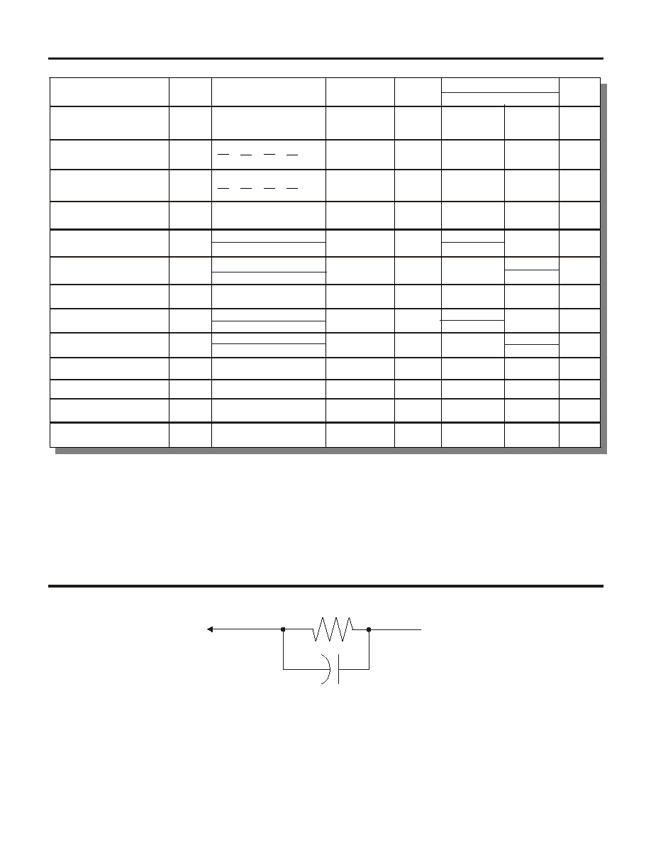
C1
C1 = 0.1 µF (±10%)
R = 1.6K
(±10%)
S1
W
G
DQ0
DIN
DQ31
A0
A16
∑
∑
∑
∑
∑
∑
∑
∑
R
R
R
R
R
R
R
128K x 32
SRAM
The dynamic
burn-in pin listing
is shown at right.
F = square wave,
100 KHz to
1.0 MHz.
Burn-In Circuit
QML Level
Comments
H
X
X
X
Sample
X
X
X
X
X
X
X
X
X
X
X
X
X
K
X
X
X
Sample
X
X
X
X
X
X
X
X
X
X
X
X
X
X
X
X
Wafer Lot Acceptance
Serialization
Flip Chip Die Pull
Destructive Bond Pull
Pre Burn-In
Electrical Test
Dynamic Burn-In 1
Electrical Test
Internal Visual
Fine and Gross Leak
Temperature Cycle
Mechanical Shock
PIND
Radiography
Electrical Test
Dynamic Burn-In 2
Final Electrical Test
PDA
Fine and Gross Leak
External Visual
Alternate Method Used
Die Traceability
MIL-STD-883, TM 2010, 2017
Bubble Test Only
Meets Group A
MIL-PRF-38534, Based On Die
MIL-STD-883, TM 2009
Flow
Input
A0
A1
A2
A3
A4
Signal
F/2
F/4
F/8
F/16
F/32
Input
A11
A12
A13
A14
A10
Signal
F/4096
F/8192
F/16384
F/32768
F/2048
Input
A6
A7
A8
A9
A5
Signal
F/128
F/256
F/512
F/1024
F/64
Signal
F/65536
V
IL
Input
W
D
IN
S1
G
A15
A16
F/131072
F/262144
F/524288
F/1048576
11
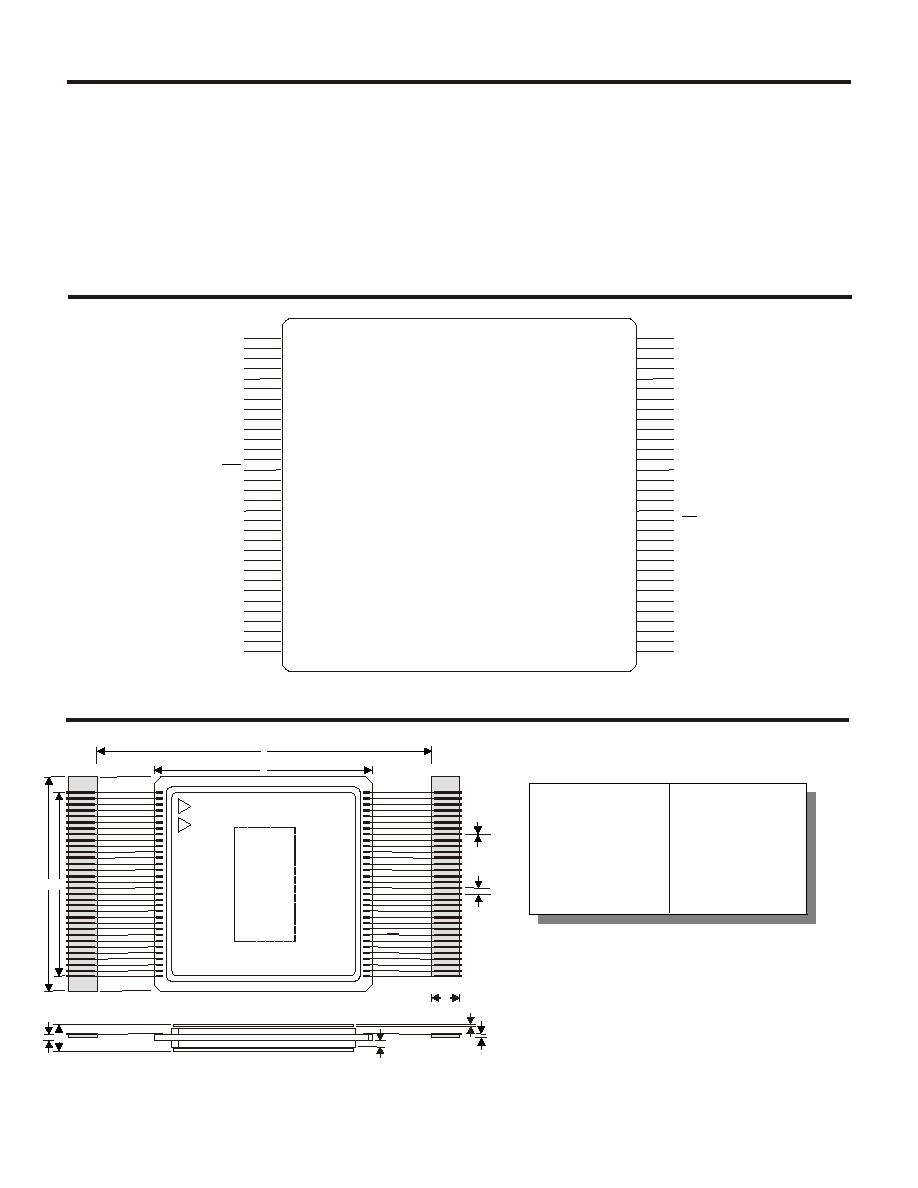
Packaging
64-Lead Dual Flat Pack Pinout
40-Lead Flat Pack
The 128K x 32 SRAM is offered in a custom 64-lead dual
FP. All packages are constructed of multilayer ceramic
(AI
2
O
3
) and feature internal power and ground planes.
Optional capacitors can be mounted to the package to
maximize supply noise decoupling and increase board
packing density. These capacitors attach directly to the
internal package power and ground planes. This design
minimizes resistance and inductance of the bond wire and
package, both of which are critical in a transient radiation
environment. All NC pins must be connected to either V
DD
,
GND or an active driver to prevent charge build up in the
radiation environment. (NC = no connect.)
Notes:
1) Part mark per device specification.
2) Dimensions are in inches.
3) Unless otherwise specified, all
tolerances are ± .005".
4) "QML" may not be required per
device specification.
A=1.760
B=1.000 ± .010
C=.900 ± .010
D=.775
E=.008 ± .002
F=.025
G=.135
H=.270 ± .012
J=.048
K=.080
1
GND
64
7
A7
A0
58
13
25
D7
A11
D15
A4
52
40
4
D2
D9
61
10
22
D4
D18
D12
D26
55
43
16
28
CS1
D20
49
37
2
D0
63
8
A1
57
14
26
WE
A12
GND
A5
51
39
5
D3
D10
60
11
23
D5
D19
D13
D27
54
42
17
29
CS4
D28
48
36
3
D1
D8
62
9
21
A9
D17
A2
D25
56
44
15
27
A14
A13
A15
50
38
6
V
DD
D11
59
12
24
D6
A10
D14
A3
53
41
18
30
A16
D22
D29
47
35
19
31
OE
D30
20
32
D16
GND
D24
D31
45
33
46
34
Top
View
Lead 1
Lead 32
(1)
Lead 64
Lead 33
J
G
F
(Pitch)
L
M
K
E
(Width)
L=.025
M=.035
D
C
B
A
H
D23
D21
CS3
A8
V
DD
GND
V
DD
CS2
V
DD
V
DD
A6
128K x 32 CMOS Memory Device - MCM (5 V)
∑Part Number 255A833
Cleared for Public Domain Release
©2001 BAE SYSTEMS, All Rights Reserved
BAE SYSTEMS ∑ 9300 Wellington Road ∑ Manassas, Virginia 20110-4122
BAE SYSTEMS
An ISO 9001, AS9000, ISO 14001,
and SEI CMM Level 4 Company
9300 Wellington Road, Manassas, VA 20110-4122
866-530-8104
http://www.baesystems-iews.com/space/
0037_128K_32_SRAM.ppt
BAE SYSTEMS reserves the right to make changes to
any products herein to improve reliability, function or
design. BAE SYSTEMS does not assume liability arising
out of the application or use of any product or circuit
described herein, neither does it convey any license
under its patent rights nor the rights of others.
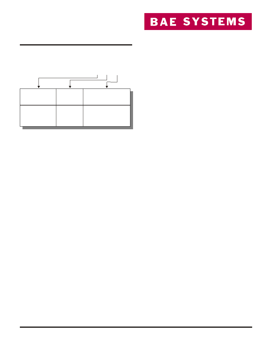
Ordering Information
X
Y
Z
Z
Screen
Designation
X
Package
Designation
1=64-Lead FP
1=Class K
3=Engineering
5=Class H
7=Customer Specific
Y
Speed
Designation
2 = 25 ns
3 = 30 ns