 | ÐлекÑÑоннÑй компоненÑ: AZ4580 | СкаÑаÑÑ:  PDF PDF  ZIP ZIP |
Äîêóìåíòàöèÿ è îïèñàíèÿ www.docs.chipfind.ru
DUAL LOW NOISE OPERATIONAL AMPLIFIERS AZ4580
1
Issue Date: Jan. 2003
Advanced Analog Circuits
Data Sheet
Rev.1.0
General Description
The AZ4580 is a dual low noise operational amplifier.
It is specifically designed for audio systems to improve
tone control; it can also be used in pre-amplifier, indus-
trial measurement tools and applications where gain
and phase matched channels are mandatory.
The IC features monolithic silicon chip, internal fre-
quency compensation, low noise, low distortion, high
gain and high bandwidth. The AZ4580 can operate
under dual power supply voltage up to
±18V or single
power supply up to 36V.
Features
·
Operating voltage:
±2V ~ ±18V
·
Large DC voltage gain: 110dB typ.
·
Low input noise voltage: 0.7
µV
RMS
typ.
·
Wide gain bandwidth product: 15 MHz typ.
·
Low distortion: 0.0005% typ.
·
Slew rate: 7V/
µs typ.
·
Package outline: DIP8, SOIC8
Applications
·
Audio AC-3 decoded system
·
Audio amplifier
SOIC-8
DIP-8
Figure 1. Package Types of AZ4580
DUAL LOW NOISE OPERATIONAL AMPLIFIERS AZ4580
2
Issue Date: Jan. 2003
Advanced Analog Circuits
Data Sheet
Rev.1.0
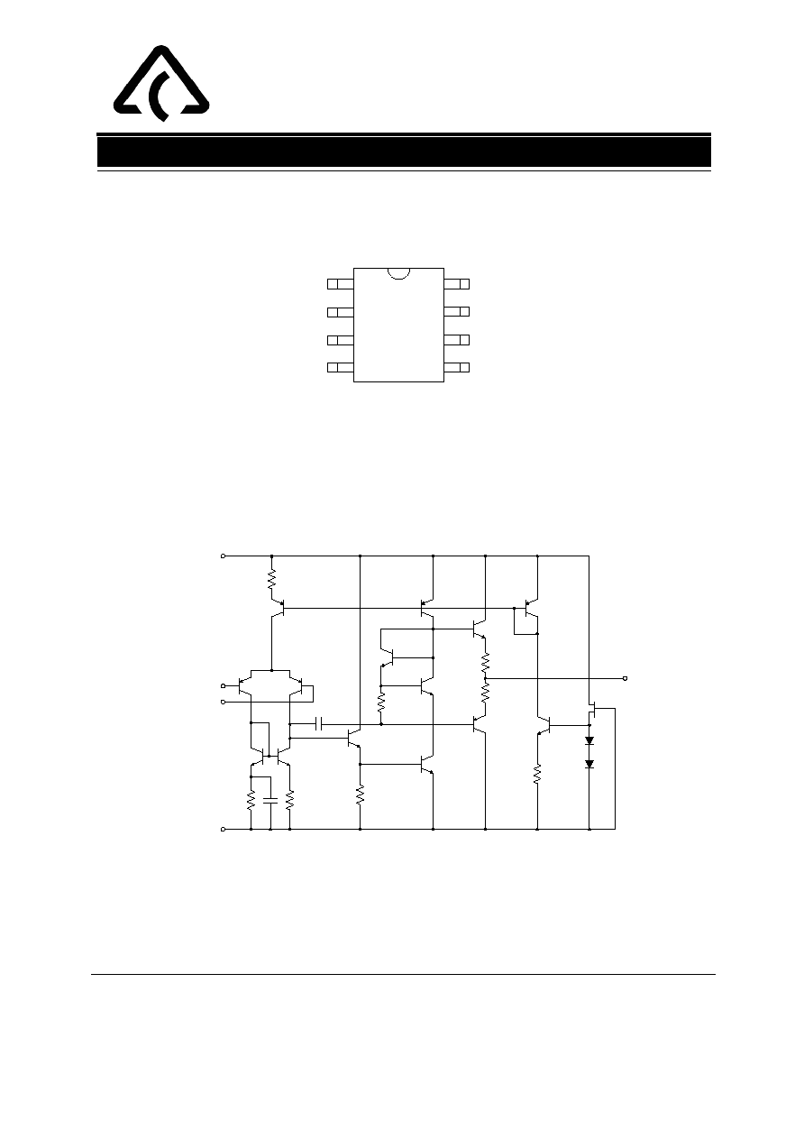
Figure 3. Representative Schematic Diagram of AZ4580
Functional Block Diagram
Pin Configuration
Figure 2. Pin configuration of AZ4580
OUTPUT 1
INPUT 1-
INPUT 1+
V
EE
V
CC
OUTPUT 2
INPUT 2-
INPUT 2+
1
4
5
6
7
8
3
2
V
CC
-INPUT
+INPUT
V
EE
OUTPUT
Top View
DUAL LOW NOISE OPERATIONAL AMPLIFIERS AZ4580
3
Issue Date: Jan. 2003
Advanced Analog Circuits
Data Sheet
Rev.1.0
Parameter
Min.
Max.
Unit
Power Supply Voltage
V
CC
+ 20
V
V
EE
- 20
Differential Input Voltage
V
ID
± 30
V
Input Voltage
V
IC
± 15
V
Power Dissipation
DIP-8
800
mW
SOIC-8
800
Operating Temperature Range
T
OP
-40 to 85
o
C
Storage Range
T
STG
-60 to 150
o
C
ESD (Human Body Mode)
4000
V
ESD (Machine Mode)
350
Absolute Maximum Ratings (Note 1)
Package
Temperature Range
Part Number
Packing Type
SOIC-8
-40
o
C to 85
o
C
4580M
Tube, Reel
DIP-8
AZ4580P
Tube
Ordering Information
Recommended Operation Conditions
Parameter
Min.
Max.
Unit
Supply Voltage
± 2
± 18
V
Note 1: Stresses greater than those listed under "Absolute Maximum Ratings" may cause permanent damage to the
device. These are stress ratings only, and functional operation of the device at these or any other conditions beyond
those indicated under "Recommended Operation Ratings" is not implied. Exposure to "Absolute Maximum Rat-
ings" for extended periods may affect device reliability.
DUAL LOW NOISE OPERATIONAL AMPLIFIERS AZ4580
4
Issue Date: Jan. 2003
Advanced Analog Circuits
Data Sheet
Rev.1.0
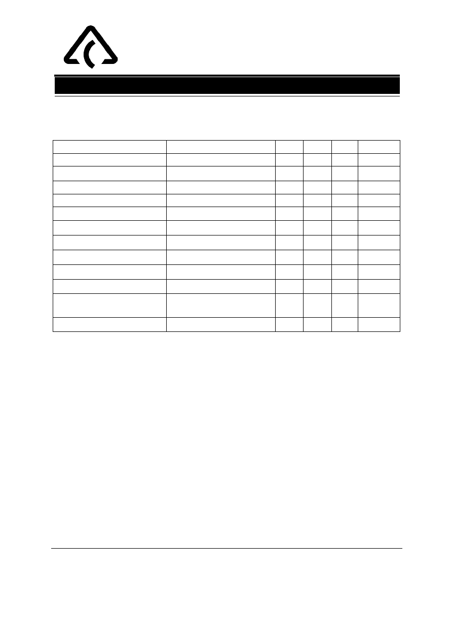
Operating Conditions: V
CC
=
+
15V, V
EE
= - 15V, T
A
= 25
o
C unless otherwise specified.
Electrical Characteristics
Parameter
Conditions
Min.
Typ.
Max.
Unit
Supply Current
no load
-
4
7
mA
Input Offset Voltage
R
S
10K
-
0.5
3
mV
Input Offset Current
-
5
100
nA
Input Bias Current
-
150
500
nA
Input Common Mode Voltage Range
±
12
±
13.5 -
V
Common Mode Rejection Ratio
V
CM
=0V to V
CC
-1.5V, R
S
10K
80
110
-
dB
Large Signal Voltage Gain
R
L
=2K
, V
O
=
±
10V
90
110
-
dB
Power Supply Rejection Ratio
R
S
10K
80
110
-
dB
Slew Rate
R
L
2K
-
7
-
V /
µ
S
Gain Bandwidth Product
R
L
=2K
, f=10KHz
-
15
-
MHz
Total Harmonic Distortion
A
V
=20dB, V
O
=5V
R
L
=2K
, f=1KHz
-
0.0005
-
%
Equivalent Input Noise Voltage
RIAA R
S
=2.2K
, 30KHz LPF
-
0.7
µV
RMS
DUAL LOW NOISE OPERATIONAL AMPLIFIERS AZ4580
5
Issue Date: Jan. 2003
Advanced Analog Circuits
Data Sheet
Rev.1.0
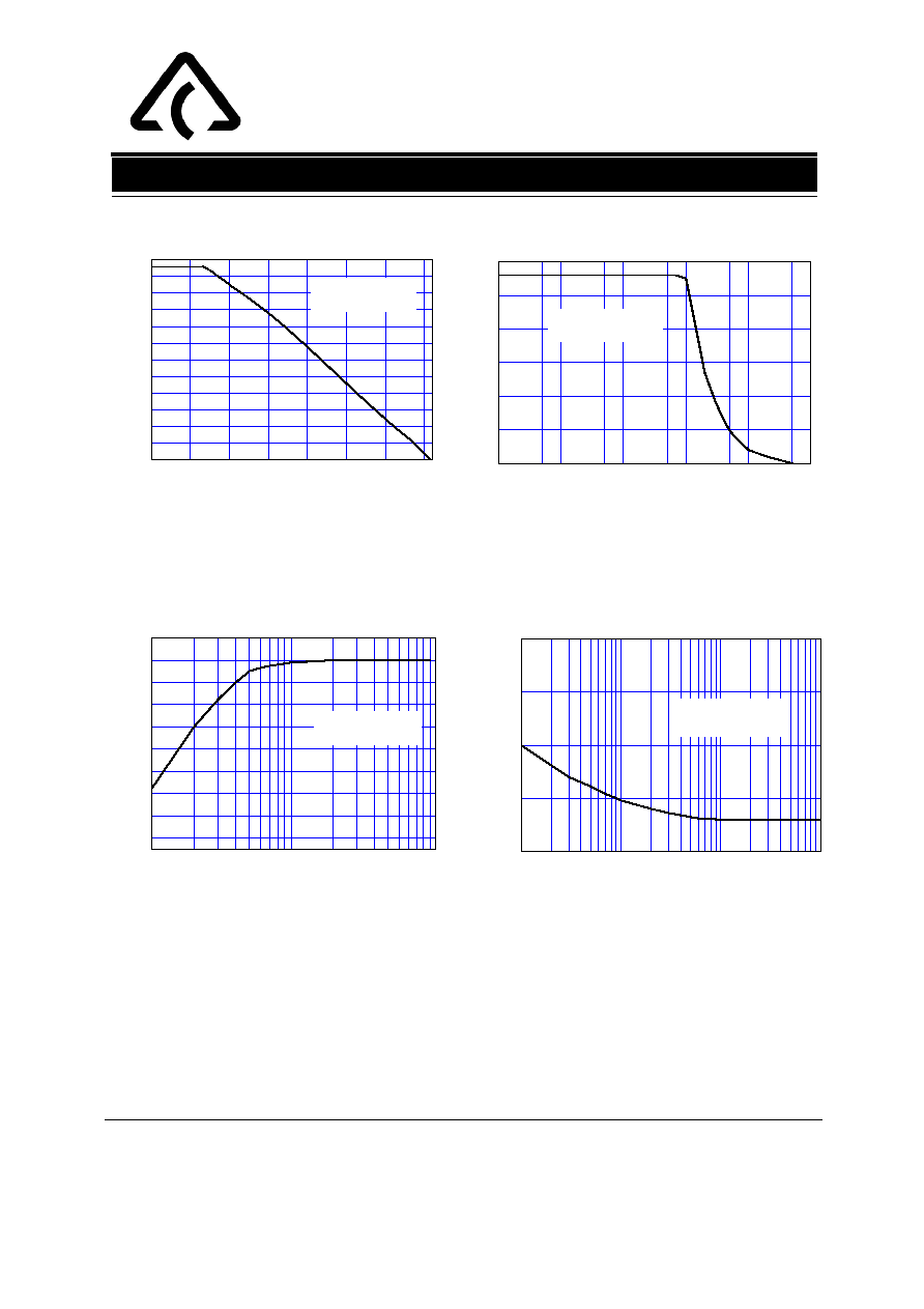
Typical Characteristics
Figure 4. Open Loop Voltage Gain
Figure 5. Maximum Output Voltage Swing
Figure 6. Maximum Output Voltage Swing
Figure 7. Equivalent Input Noise Voltage
vs. Frequency
vs. Load Resistance
vs. Frequency
1
10
100
1k
10k
100k
1M
10M
0
10
20
30
40
50
60
70
80
90
100
110
120
V
CC
= 15V, V
EE
= -15V
R
L
=2K
,T
A
=25
o
C
Ope
n
Loop V
o
lt
age G
a
in (dB
)
Frequency (Hz)
vs.
100
1k
10k
100k
1M
10M
0
5
10
15
20
25
30
O
u
t
p
ut
V
o
lt
ag
e S
w
in
g
(
V
)
Frequency (H z)
V
CC
= 15V,V
EE
= -15V
R
L
=2K
, T
A
=25
o
C
0.1
1
10
12
14
16
18
20
22
24
26
28
30
V
CC
= 15V,V
EE
= -15V,
T
A
=25
o
C
O
u
tput
Vo
lt
a
ge Swing (V)
Load Resistance (K
)
Frequency
1
10
100
1k
0
5
10
15
20
Frequency (Hz)
E
q
u
i
va
le
nt
I
n
pu
t
No
i
s
e V
o
l
t
age
(
n
V
/
(
H
z
)
0.
5
)
V
CC
= 15V, V
EE
= -15V
R
S
=50
,T
A
=25
o
C