L
Q
QT60040
4-K
EY
C
HARGE
-T
RANSFER
IC
Creates 4 `touch buttons' through any dielectric
Only 1 inexpensive capacitor required
Simple 4x1 matrix key geometry
100% drift compensation for lifetime reliability
'2' key rollover: senses any 2 keys at same time
Back-lit keys possible with ITO electrodes
Simple direct 'per key' active-high drive outputs
Auto recalibration after 10 or 60 seconds of touch
2.5 - 5.5V single power supply operation
CMOS design - very low power consumption
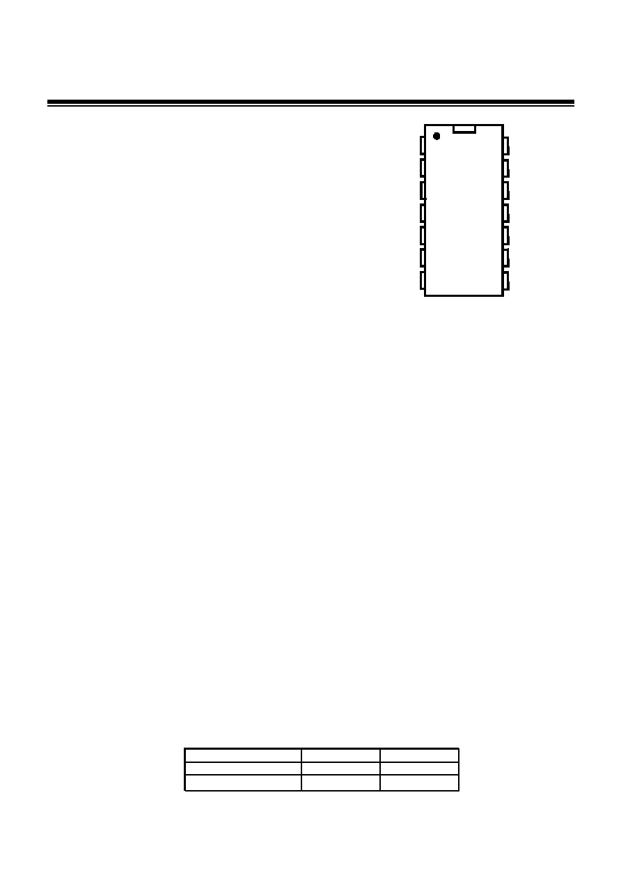
14-pin SOIC package
E604 Evaluation reference design board available
APPLICATIONS -
Automotive controls
PC / peripheral controls
ATM machines
Touch-screens
Appliance controls
Vandal-proof keypads
Security keypanels
Industrial keyboards
The QT60040 digital charge-transfer ("QT") QMatrixTM IC is designed to detect touch on up to 4 keys in a scanned 4x1 matrix.
It will project the keys through almost any dielectric, like glass, plastic, stone, ceramic, and even most kinds of wood, up to
thicknesses of 6mm. The touch areas are defined as simple 2-part interdigitated electrodes of conductive material, like
copper, Indium-Tin-Oxide (ITO), or screened silver or carbon deposited on the rear of a control panel. Alternatively the keys
can be implemented on a stick-on flex circuit that can be adhered to the rear of most panels.
The IC is designed specifically for domestic appliances, computer and peripheral control buttons, ATM machines, security
panels, portable instruments, machine tools, or similar products that are subject to environmental challenges or physical
attack. It permits the construction of 100% sealed, watertight keypanels that are immune to environmental factors such as
humidity and condensation, temperature, dirt accumulation, or the physical deterioration of the panel surface from abrasion,
chemicals, or abuse. The QT60040 contains Quantum-pioneered self-calibration, drift compensation, and digital filtering
algorithms that make its sensing function extremely robust and survivable.
The device can easily control keys over graphical LCD panels or LEDs when used with clear, conductive ITO electrodes. It
does not require 'chip on glass' or other exotic fabrication techniques, thus allowing the OEM to source the keymatrix from
multiple vendors.
External circuitry consists only of a single, inexpensive capacitor. The sensitivity of the keys can be set by simply changing
the value of this capacitor. The device has 4 outputs which indicate detection on the keys; up to 2 keys can be sensed at any
one time.
The QT60040 features automatic recalibration timeouts which will cause the device to recalibrate keys on an individual basis
when they are 'stuck on' for intervals of either 10s or 60s, depending on a jumper option.
QT60040 technology makes use of an important new variant of charge-transfer sensing, transverse charge-transfer, in an XY
format that minimizes the number of required scan lines and external components. Unlike older technologies it does not
require one IC per key, and is cost competitive even with some rubber membrane technologies. A distinct advantage is an
accelerated time to market due to the fact that custom molded membranes are not required; the entire system can be
designed using common PCB materials.
The E604 board available from Quantum is a reference design that permits full evaluation of the QT60040
lQ
Copyright � 2000 Quantum Research Group Ltd
QT60040 / R1.04 / 0303
X1
OPT1
OPT2
Q1
Q2
Q3
Q4
CS
Y
X4
X3
X2
1
2
3
4
5
6
7
8
9
10
11
12
13
14
VDD
GND
-
QT60040-IS
-40
0
C to +85
0
C
QT60040-D
-
0
0
C to +70
0
C
DIP
SOIC
T
A
AVAILABLE OPTIONS

1 - OVERVIEW
The QT60040 is a CMOS charge-transfer (QT) sensor designed
specifically for matrix touch controls; it includes all signal
processing functions necessary to provide stable sensing under a
wide variety of changing conditions. Only one low cost external
capacitor is required for operation.
The QT60040 uses burst-mode charge transfer methods
pioneered and patented by Quantum. This revolutionary new
technology allows the construction of entirely new forms of
keypanels which can include back-illumination, arbitrary shapes
of keys, 'morphed' keys wrapped onto complex surfaces, and
keys having unique textures and feel, all at very low cost.
The QT60040 uses a 4x1 matrix, having 4 'X' drive lines and 1 'Y'
receive line. This configuration reduces interconnect
requirements and also lowers the external component count to
one charge sampling capacitor which is sequentially shared by
the four keys.
The QT60040 has four simple active-high CMOS outputs that go
high when the corresponding key is touched. Up to 2 keys can be
touched at the same time; three or more keys touched will limit to
the first two touch outputs. An option pin allows this to be
restricted to only one key if desired.
The device operates on a 2.5 to 5.5 regulated power supply
which can be from a common 78L05-type IC regulator or a simple
2-stage zener regulator supply.
1.1 FIELD FLOWS
Figure 1-1 shows how charge is transferred across an electrode
set to permeate the overlying panel material; this charge flow
exhibits a rapid dQ/dt during the edge transitions of the X drive
pulse. The charge emitted by the X electrode is partly received
onto the Y electrode which is then captured by the Cs capacitor
and processed.
The QT60040 matrix uses 4 'X' edge-driven rows and 1 'Y' sense
column to detect 4 keys. The X drive occurs as a burst of pulses
on each key.
The charge flows set into motion by the X drive signals are
partially absorbed by the touch of a human finger (Figure 1-2)
resulting in a decrease in coupling from X to Y; coupled charge
increases in the presence of a conductive film like water (Figure
1-3) which acts to bridge the two elements. Increasing signals
due to water films are quite easy to discern and are not detected
by the QT60040.
1.2 CIRCUIT MODEL
An electrical circuit model is shown in Figure 1-4. The coupling
capacitance across the X and Y electrodes and from each to a
finger is represented by Cx1, Cx2a, and Cx2b. The sampling
capacitor Cs is used to accumulate charge during the course of a
burst. An important parasitic capacitance from the Y line to
ground, Cx3, is also shown.
QT switch timing action is shown in Figure 1-5.
Initially, switch S3 is closed to reset Cs then re-opened. After S3
is opened, S1 is closed to charge the capacitances associated
with the Y-line, including all Y-to-X capacitances. After S1 is
closed, one of the four X lines is raised high, so that there is then
a zero differential potential from the selected X line to the Y line.
Then, S1 is opened and S2 is closed, causing charge to flow
from the Cx capacitances into Cs; Cs charges up slightly with the
polarity shown. Then the selected X line is driven low, causing a
step-function decrease in charge on Cs whose magnitude is
proportionate to the amount of coupling from X to Y.
The final charge accumulated on Cs per QT cycle is thus a direct
function of Cx3 minus the small amount of charge subtracted via
the Cx1 / Cx2a / Cx2b / Cfinger network. Since the charge from
the Cx2a / Cx2b network is highly dependent on Cfinger, which
effectively forms a capacitive divider, the total charge absorbed
by Cs is dependent on touch: a touch nets more charge
transferred into Cs per QT cycle because less charge is
transferred out of Cs per QT cycle.
The acquisition process is controlled by a state machine which
continues the acquisition cycle as a burst, which finally
terminates when the voltage across Cs reaches the predefined
level Vref. This burst takes hundreds or even thousands of cycles
�Quantum Research Group Ltd.
lQ
- 2 -
QT60040 / R1.04 / 0303
Figure 1-2 Field Flows When Touched
Figure 1-3 Fields With a Conductive Film
cm os
driver
overly ing panel
X
element
Y
elem ent
Water film
Figure 1-1 Field flow between X and Y elements
cmos
driver
overlying panel
X
element
Y
element
to complete; the burst length depends on the value of Cs, the Cx
capacitances, and Cfinger. Increasing Cs increases the burst
length, increasing Cx3 decreases burst length, and increasing
Cx1 and Cx2 increase burst length. Increasing Cfinger decreases
the burst length. The value of the burst length is thus a variable
that is dependent on these capacitances; the burst length is used
to create an internal reference signal level during a calibration
cycle, and to determine the presence of touch by virtue of a
change in the burst length relative to the reference level.
Because the Cs capacitor is shared among all four channels it is
important that the four interdigitated key designs be reasonably
well matched. It is also important to keep Cx1 and Cx3 to a
minimum while maximizing the values of Cx2a and Cx2b through
good key design methods. These requirements also dictate that
the IC be placed close to the keys to achieve good sensitivity
levels; long Y traces also increase the risk of susceptibility to
interference, as well as low gain. To reduce Cx3, the Y line
should not be run close to other unrelated traces or over or near
ground planes.
1.3 SINGLE ELECTRODE OPERATION
An alternative mode of operation is shown in Figure 1-6.
Capacitances Cx2a and Cx2b are implemented as discrete
capacitances, possibly by using intentional mutual capacitive
coupling of tracks on a PCB; traces from the intersections of
these capacitors are led to solid touch pads which are
implemented as metallizations on the rear of a control panel.
Touching the front of the panel has the same absorptive effect on
signal strength as an interdigitated electrode set.
The values of Cx2a and Cx2b should be consistent among all
keys to preserve signal balance, which is required for proper
operation. The surface area and geometry of this type of
electrode should be adjusted to suit the desired activation area.
Typical values of Cx2a and Cx2b range from 5pF to 10pF. The
traces leading from the junctions of these capacitors to the solid
touch pads should not see a load of more than 10pF, thus the
traces to these pads should be thin and short and not
accompanied by a ground plane or other traces.
1.4 INTERDIGITATED ELECTRODES
Key electrodes can be made using interdigitated sets of fingers,
serpentines, spirals or similar patterns (Figure 1-7). One element
of each key must be connected to an X line, with the other
connected to the common Y line. The pattern surface area should
be similar from key to key to preserve relative key sensitivities.
It is important to prevent substantial capacitive coupling from a
`bare' Y line to a finger. A transient increase in Cx3 will cause a
sudden disturbance common to all keys that can create
unintentional detections. The connecting Y trace running between
the keys should be as thin as possible, on a side of the flex circuit
or pcb away from the user panel, and where possible run closely
in parallel with a segment of a nearby X trace so as to suppress
this effect. The problem of a bare Y line can be demonstrated by
touching the Cs capacitor (which is connected to Y), which will
cause one or two random keys to activate with each touch.
In cases where it is not possible to have both the X and Y traces
on the same plane, the X traces should be run on the `finger' side
of the board. In all cases where the X and Y lines run on opposite
planes, the substrate (a flex circuit, or a pcb) should be as thin as
�Quantum Research Group Ltd.
lQ
- 3 -
QT60040 / R1.04 / 0303
Figure 1-4 QT60040 Circuit Model
Figure 1-5 Circuit Switch Timings
RE SET S 3
Cycle 'm '
V REF
X DRIV E X
n
CH ARG E S 1
TR ANS FER S 2
V
C S
C ycle 1
S3
RESET
S1
CHARGE
S2
TRANSFER
C
STATE
MACHINE
POST
PROCESSOR
DONE
START RESULT
OUT
OPTIONS
Vref
X
DRIVE
n
C
FINGER
C
X2A
C
X2B
C
X1
C
X3
C
S
+ -
1 OF 4
Figure 1-6 Conversion to Single Electrodes
C
X 2 B
C
FIN G E R
X 1
X 2
X 3
X 4
C
S
Y
QT60040
C
X 2 A
Figure 1-7 Sample Electrode Geometries
PARALLEL LINES
SERPENTINE
SPIRAL
possible to promote equal field coupling through the overlying
panel material and to increase sensitivity.
Suggested design rules for interdigitated keys are shown in
Figure 1-8.
1.5 SIGNAL PROCESSING
The QT60040 calibrates and processes all signals using a
number of algorithms pioneered by Quantum. These algorithms
are specifically designed to survive most environmental
conditions.
1.5.1 S
ELF
-C
ALIBRATION
The QT60040 is fully self-calibrating. On powerup it scans the
matrix and sets appropriate calibration points for each. No special
operator or factory calibration or circuit tweak is required to bring
keys into operation. The self calibration procedure typically
requires 1 second to complete.
1.5.2 D
RIFT
C
OMPENSATION
A
LGORITHM
Signal drift can occur because of changes in Cx and Cs over
time. It is crucial that drift be compensated for, otherwise false
detections, non-detections, and sensitivity shifts will follow.
Drift compensation (Figure 1-9) is performed by making the
reference level track the raw signal at a slow rate, but only while
there is no detection in effect. The rate of adjustment is
performed slowly, otherwise legitimate detections might be
ignored. The QT60040 drift compensates using a slew-rate
limited change to the reference level; the threshold and
hysteresis values are slaved to this reference.
The QT60040's drift compensation is 'asymmetric': the
drift-compensation occurs in one direction faster than it does in
the other. Specifically, it compensates faster for decreasing
loads. Increasing loads (more contact with an object, which
results in a decreasing signal) should be compensated for slowly,
so that sensitivity to an approaching finger is not affected.
Removal of an object is compensated for at a faster rate to allow
the sensor to recover quickly to prepare for the next valid touch.
1.5.3 T
HRESHOLD
AND
H
YSTERESIS
C
ALCULATIONS
The threshold value is established as an offset to the reference
level. As Cx and Cs drift over time, the reference drift
compensates with the changes and the threshold level is
automatically recomputed in real time so that it is never in error.
Since key touches result in negative signal swings, the threshold
is set below the signal reference level.
The QT60040 employs a hysteresis of 25% of the delta between
the reference and threshold levels. The signal must rise by 25%
of the distance from threshold to reference before the detection
event drops out and the key registers as untouched.
1.5.4 M
AX
O
N
-D
URATION
If a foreign object contacts a key the signal may
change enough to create a detection lasting for the
duration of the contact. To overcome this, the part
includes individual key timers which monitor detection
duration. If a detection on a key exceeds the timer limit
setting, the sensor will perform a full recalibration. This
is known as the Max On-Duration feature.
After the Max On-Duration interval has expired and the
recalibration has taken place, the key will once again
function normally even if still in contact with the foreign
object, to the best of its ability. The Max On-Duration
can be set to either 10 or 60 seconds of continuous
detection by a jumper option (Table 2-1); this option applies to all
keys.
Max On-duration has no interaction among keys; a timeout on
one key will have no effect on another key.
1.5.5 D
ETECTION
I
NTEGRATOR
To suppress false detections caused by spurious events like
electrical noise, the QT60040 incorporates a detection integration
counter that increments with each detection sample until a limit is
reached, at which point a detection is confirmed. If no detection is
sensed on any of the samples prior to the final count, the counter
is reset immediately to zero, forcing the process to restart. The
required count is 3 samples per key.
�Quantum Research Group Ltd.
lQ
- 4 -
QT60040 / R1.04 / 0303
Figure 1-8 Key Design Rules
0.75mm
gaps
0.5mm
lines
X shield
tails
Common
Y Line
X1
X2
18x18mm
key size
Figure 1-9 Drift Compensation
Threshold
Signal
Hysteresis
Reference
Output

2 - CIRCUIT SPECIFICS
The basic QT60040 circuit is shown in Figure 2-1.
2.1 C
S
CAPACITOR
The QT60040 requires only a single external sampling capacitor
(Cs) to operate. This capacitor should have good stability
characteristics. It is possible but not optimal to use an X7R type
capacitor, but for best stability a plastic type such as polyester or
PPS film should be used. Increasing values will result in
increased sensitivity, but too much sensitivity can also result in
spurious operation. The optimal value of Cs will depend on the
type of panel material, its thickness, and key geometry;
experimentation is required to determine the proper value.
Typical suitable values of Cs range from 22nF to 220nF; 47nF is
a good value to start from in most cases.
2.2 OPTION PINS
There are two option pins whose function is shown in Table 2-1.
OPT1 is used to set the rollover option. If this pin is connected to
ground, the IC will only sense one key at a time. If OPT1 is left
open or connected to Vdd, the IC can sense any two keys
simultaneously and will suppress additional keys.
OPT2 is used to set the calibration time-out function. If OPT2 is
connected to ground, keys will time out and recalibrate after 10
seconds of continuous detection on a key. If OPT2 is left open or
connected to Vdd, keys will recalibrate after 60 seconds. In either
case the keys will continue to be functional after the time-out, to
increased amounts of finger touch.
2.3 POWER SUPPLY
The IC uses the power supply rail as an internal reference
voltage. If the power supply is shared with another electronic
system, care should be taken to assure that the supply is free of
digital spikes, sags, and surges which can adversely affect the
circuit. The QT60040 will track slow changes in Vcc, but it can be
adversely affected by rapid voltage steps and impulse noise on
the supply rail.
The power supply can range from +2.5 to +5.5 volts, and should
be regulated via a standard regulator such as a 78L05 type. In
cases where low cost is an objective, it is possible to use
double-zener regulation.
For proper operation a 100nF (0.1uF) ceramic bypass capacitor
should be used between Vdd and Vss; the bypass cap should be
placed very close to the device's power pins.
2.4 OUTPUTS
The device has four active-high outputs, one per sensing
channel, which indicate touch. These outputs should be used for
logic-level switching only and should not drive loads of more than
1mA. High loads can cause shifts in device Vdd and Vss rails
which can lead to spurious operation.
2.5 ESD PROTECTION
In general the QT60040 will be protected from direct static
discharge by the overlying panel. However, even with a panel,
transients can still flow into the electrode via induction, or in
extreme cases, via dielectric breakdown. Porous or thin materials
may allow a spark to tunnel right through the panel material.
Testing is required to reveal any problems. The QT60040 does
have diode protection on its terminals which can absorb and
protect the device from most induced discharges, up to 20mA;
the usefulness of the internal clamping will depend on the
dielectric properties, panel thickness, rise time of the ESD
transients, and their duration.
The device pins can be further protected by inserting series
resistance into the X and Y lines. The resistances chosen should
not be so high as to interfere with the QT process. Every board
layout is different and thus it is difficult to specify a suitable value,
however, typical values will range from 1K ohms to 47K ohms. In
serious cases additional low-capacitance high-conductance
clamp diodes (e.g. BAV99) may be added to shunt ESD aside
from the X and Y pins to the power and ground rails.
The QT60040's 'X' drive lines are always being driven at low
impedance; they are never 3-state unless the circuit is just
powering up or is powered down. This is a considerable
advantage in dealing with ESD. The 4 output pins may also be
vulnerable and should be resistor and/or diode protected if they
are in danger of being subject to ESD.
�Quantum Research Group Ltd.
lQ
- 5 -
QT60040 / R1.04 / 0303
Figure 2-1 Basic Circuit Diagram
Cs
QT
6
0040
X1
Q1
Opt1
Y
Cs
X2
Q2
Opt2
X3
Q3
X4
Q4
2
13
12
11
10
9
3
4
5
6
7
8
14
1
Vdd
Vss
A
C
TI
V
E-
H
I
G
H
OUTPUT
S
OP
T
I
O
N
S
KEY
S
+5
M1
M2
M3
M4
10 seconds to recalibration
Vss
60 seconds to recalibration
Vdd
Pin 4
OPT2
1 key only can be sensed
Vss
2 keys can be sensed
Vdd
Pin 3
OPT1
Table 2-1 Option Pin Functions