
18
y 0x79 - Column Keys Scope
. . . . . . . . . . . . . . . . . . . . . . . . . . .
18
x 0x78 - Row Keys Scope
. . . . . . . . . . . . . . . . . . . . . . . . . . . . .
18
S 0x53 - All Keys Scope
. . . . . . . . . . . . . . . . . . . . . . . . . . . . . .
18
s 0x73 - Specific Key Scope
. . . . . . . . . . . . . . . . . . . . . . . . . . .
18
5.2 Scope Commands
. . . . . . . . . . . . . . . . . . . . . . . . . . . . . .
17
p 0x70 - Put Command
. . . . . . . . . . . . . . . . . . . . . . . . . . . . . .
17
g 0x67 - Get Command
. . . . . . . . . . . . . . . . . . . . . . . . . . . . . .
17
5.1 Put / Get Direction Commands
. . . . . . . . . . . . . . . . . . . . .
17
5 Commands & Functions
. . . . . . . . . . . . . . . . . . . . . . . . . . . . .
16
4.8 Eeprom Corruption
. . . . . . . . . . . . . . . . . . . . . . . . . . . . . .
15
4.7 Parallel Scan Port
. . . . . . . . . . . . . . . . . . . . . . . . . . . . . . .
15
4.6 Sensor Echo and Data Response
. . . . . . . . . . . . . . . . . .
14
4.5 UART Interface
. . . . . . . . . . . . . . . . . . . . . . . . . . . . . . . . .
13
4.4 SPI Master-Slave Mode
. . . . . . . . . . . . . . . . . . . . . . . . . .
12
4.3 SPI Slave-Only Mode
. . . . . . . . . . . . . . . . . . . . . . . . . . . .
12
4.2 SPI Port Specifications
. . . . . . . . . . . . . . . . . . . . . . . . . . .
11
4.1 Serial Protocol Overview
. . . . . . . . . . . . . . . . . . . . . . . . . .
11
4 Communications Interfaces
. . . . . . . . . . . . . . . . . . . . . . . . . .
11
3.18 ESD / Noise Considerations
. . . . . . . . . . . . . . . . . . . . . .
11
3.17 Power Supply & PCB Layout
. . . . . . . . . . . . . . . . . . . . .
11
3.16 Oscilloscope Sync
. . . . . . . . . . . . . . . . . . . . . . . . . . . . . .
10
3.15 LED / Alert Output
. . . . . . . . . . . . . . . . . . . . . . . . . . . . . .
9
3.14 Sleep_Wake / Noise Sync Pin (WS)
. . . . . . . . . . . . . . . . .
9
3.13 Startup / Calibration Times
. . . . . . . . . . . . . . . . . . . . . . . . .
9
3.12 Oscillator
. . . . . . . . . . . . . . . . . . . . . . . . . . . . . . . . . . . . . . .
9
3.11 Reset Input
. . . . . . . . . . . . . . . . . . . . . . . . . . . . . . . . . . . . .
9
3.10 Water Film Suppression
. . . . . . . . . . . . . . . . . . . . . . . . . . .
9
3.9 Sample Capacitors
. . . . . . . . . . . . . . . . . . . . . . . . . . . . . . . .
9
3.8 Burst Spacing
. . . . . . . . . . . . . . . . . . . . . . . . . . . . . . . . . . . .
9
3.7 Intra-Burst Spacing
. . . . . . . . . . . . . . . . . . . . . . . . . . . . . . . .
8
3.6 Burst Acquisition Duration
. . . . . . . . . . . . . . . . . . . . . . . . . .
8
3.5 Burst Length & Sensitivity
. . . . . . . . . . . . . . . . . . . . . . . . . . .
8
3.4.2 Noise Coupling Into Y Lines
. . . . . . . . . . . . . . . . . . . . . . . . . . . .
8
3.4.1 RFI From Y Lines
. . . . . . . . . . . . . . . . . . . . . . . . . . . . . . . . . .
8
3.4 'Y' Gate Drives
. . . . . . . . . . . . . . . . . . . . . . . . . . . . . . . . . . . .
8
3.3.2 Noise Coupling Into X lines
. . . . . . . . . . . . . . . . . . . . . . . . . . . .
8
3.3.1 RFI From X Lines
. . . . . . . . . . . . . . . . . . . . . . . . . . . . . . . . . .
8
3.3 'X' Electrode Drives
. . . . . . . . . . . . . . . . . . . . . . . . . . . . . . . .
7
3.2 Signal Path
. . . . . . . . . . . . . . . . . . . . . . . . . . . . . . . . . . . . . .
7
3.1 Matrix Scan Sequence
. . . . . . . . . . . . . . . . . . . . . . . . . . . . .
7
3 Circuit Operation
. . . . . . . . . . . . . . . . . . . . . . . . . . . . . . . . . . . . .
7
2.11 Device Status & Reporting
. . . . . . . . . . . . . . . . . . . . . . . . .
7
2.10 Full Recalibration
. . . . . . . . . . . . . . . . . . . . . . . . . . . . . . . . .
6
2.9 Adjacent Key Suppression (`AKS')
. . . . . . . . . . . . . . . . . . . .
6
2.8 Reference Guardbanding
. . . . . . . . . . . . . . . . . . . . . . . . . . .
6
2.7 Positive Recalibration Delay
. . . . . . . . . . . . . . . . . . . . . . . . .
6
2.6 Detection Integrator
. . . . . . . . . . . . . . . . . . . . . . . . . . . . . . . .
6
2.5 Negative Recalibration Delay
. . . . . . . . . . . . . . . . . . . . . . . .
5
2.4 Drift Compensation
. . . . . . . . . . . . . . . . . . . . . . . . . . . . . . . .
5
2.3 Hysteresis
. . . . . . . . . . . . . . . . . . . . . . . . . . . . . . . . . . . . . . .
5
2.2 Positive Threshold
. . . . . . . . . . . . . . . . . . . . . . . . . . . . . . . . .
5
2.1 Negative Threshold
. . . . . . . . . . . . . . . . . . . . . . . . . . . . . . . .
5
2 Signal Processing
. . . . . . . . . . . . . . . . . . . . . . . . . . . . . . . . . . . .
4
1.3 Communications
. . . . . . . . . . . . . . . . . . . . . . . . . . . . . . . . . .
4
1.2 Circuit Overview
. . . . . . . . . . . . . . . . . . . . . . . . . . . . . . . . . .
4
1.1 Field Flows
. . . . . . . . . . . . . . . . . . . . . . . . . . . . . . . . . . . . . . .
4
1 Overview
. . . . . . . . . . . . . . . . . . . . . . . . . . . . . . . . . . . . . . . . . . . .
34
8 Index
. . . . . . . . . . . . . . . . . . . . . . . . . . . . . . . . . . . . . . . . . . . . .
33
7.2 Marking
. . . . . . . . . . . . . . . . . . . . . . . . . . . . . . . . . . . . . . .
33
7.1 Dimensions
. . . . . . . . . . . . . . . . . . . . . . . . . . . . . . . . . . . .
33
7 Mechanical
. . . . . . . . . . . . . . . . . . . . . . . . . . . . . . . . . . . . . . . .
32
6.5 Maximum Drdy Response Delays
. . . . . . . . . . . . . . . . . .
31
6.4 Protocol Timing
. . . . . . . . . . . . . . . . . . . . . . . . . . . . . . . . .
31
6.3 DC Specifications
. . . . . . . . . . . . . . . . . . . . . . . . . . . . . . .
31
6.2 Recommended operating conditions
. . . . . . . . . . . . . . . .
31
6.1 Absolute Maximum Specifications
. . . . . . . . . . . . . . . . . .
31
6 Electrical Specifications
. . . . . . . . . . . . . . . . . . . . . . . . . . . .
30
5.8 Erratta / Notes
. . . . . . . . . . . . . . . . . . . . . . . . . . . . . . . . .
30
5.7 Timing Limitations
. . . . . . . . . . . . . . . . . . . . . . . . . . . . . .
27
5.6 Function Summary Table
. . . . . . . . . . . . . . . . . . . . . . . . .
26
^W 0x17 - Noise Sync
. . . . . . . . . . . . . . . . . . . . . . . . . . . . . . .
26
^R 0x12 - Oscilloscope Sync
. . . . . . . . . . . . . . . . . . . . . . . . . . .
25
^Q 0x11 - Data Rate Selection
. . . . . . . . . . . . . . . . . . . . . . . . . .
25
Z 0x5A - Enter Sleep
. . . . . . . . . . . . . . . . . . . . . . . . . . . . . . . .
25
W 0x57 - Return Part Signature
. . . . . . . . . . . . . . . . . . . . . . . . .
25
V 0x56 - Return Part Version
. . . . . . . . . . . . . . . . . . . . . . . . . . .
25
r 0x72 - Reset Device
. . . . . . . . . . . . . . . . . . . . . . . . . . . . . . .
25
l 0x6C - Return Last Command Character
. . . . . . . . . . . . . . . . . . .
24
b 0x62 - Recalibrate Keys
. . . . . . . . . . . . . . . . . . . . . . . . . . . . .
24
L 0x4C - Lock Reference Levels
. . . . . . . . . . . . . . . . . . . . . . . . .
24
6 0x36 - Eeprom Checksum
. . . . . . . . . . . . . . . . . . . . . . . . . . .
24
5.5 Supervisory / System Functions
. . . . . . . . . . . . . . . . . . . .
24
^P 0x10 - Adjacent Key Suppression (`AKS')
. . . . . . . . . . . . . . . . . .
23
^O 0x0F - Negative Reference Error Band
. . . . . . . . . . . . . . . . . . .
23
^N 0x0E - Positive Reference Error Band
. . . . . . . . . . . . . . . . . . . .
23
^M 0x0D - Intra-Burst Pulse Spacing
. . . . . . . . . . . . . . . . . . . . . . .
23
^L 0x0C - Negative Recalibration Delay
. . . . . . . . . . . . . . . . . . . . .
23
^K 0x0B - Positive Recalibration Delay
. . . . . . . . . . . . . . . . . . . . .
22
^J 0x0A - Negative Detect Integrator Limit
. . . . . . . . . . . . . . . . . . .
22
^I 0x09 - Positive Drift Compensation Rate
. . . . . . . . . . . . . . . . . .
22
^H 0x08 - Negative Drift Compensation Rate5
. . . . . . . . . . . . . . . . .
22
^G 0x07 - Burst Spacing
. . . . . . . . . . . . . . . . . . . . . . . . . . . . . .
21
^F 0x06 - Burst Length
. . . . . . . . . . . . . . . . . . . . . . . . . . . . . . .
21
^D 0x04 - Positive Threshold Hysteresis
. . . . . . . . . . . . . . . . . . . . .
21
^C 0x03 - Negative Threshold Hysteresis
. . . . . . . . . . . . . . . . . . . .
21
^B 0x02 - Positive Detect Threshold
. . . . . . . . . . . . . . . . . . . . . . .
21
^A 0x01 - Negative Detect Threshold
. . . . . . . . . . . . . . . . . . . . . . .
21
5.4 Setup Commands
. . . . . . . . . . . . . . . . . . . . . . . . . . . . . .
20
k 0x6B - Reporting of First Touched Key
. . . . . . . . . . . . . . . . . . . .
20
E 0x45 - Error Codes for Group
. . . . . . . . . . . . . . . . . . . . . . . . .
19
e 0x65 - Error Code for Selected Key
. . . . . . . . . . . . . . . . . . . . . .
19
% 0x25 - Detect Integrator Counts for Group
. . . . . . . . . . . . . . . . .
19
" 0x22 - Reference Levels for Group
. . . . . . . . . . . . . . . . . . . . . .
19
! 0x21 - Delta Signals for Group
. . . . . . . . . . . . . . . . . . . . . . . . .
19
<sp> 0x20 - Signal Levels for Group
. . . . . . . . . . . . . . . . . . . . . . .
19
7 0x37 - General Device Status
. . . . . . . . . . . . . . . . . . . . . . . . . .
18
6 0x36 - Eeprom Checksum
. . . . . . . . . . . . . . . . . . . . . . . . . . .
18
5 0x35 - Detection Integrator Counts
. . . . . . . . . . . . . . . . . . . . . .
18
2 0x32 - Reference Value
. . . . . . . . . . . . . . . . . . . . . . . . . . . . .
18
1 0x31 - Delta Signal for Single Key
. . . . . . . . . . . . . . . . . . . . . . .
18
0 0x30 - Signal for Single Key
. . . . . . . . . . . . . . . . . . . . . . . . . .
18
5.3 Status Commands
. . . . . . . . . . . . . . . . . . . . . . . . . . . . . . .
©Quantum Research Group Ltd.
lQ
ii
www.qprox.com QT60161B / R1.03
Contents
1 Overview
QMatrix devices are digital burst mode charge-transfer (QT)
sensors designed specifically for matrix geometry touch
controls; they include all signal processing functions
necessary to provide stable sensing under a wide variety of
changing conditions. Only a few low cost external parts are
required for operation. The entire circuit can be built in under
6 square centimeters of PCB area.
The device has a wide dynamic range that allows for a wide
variety of key sizes and shapes to be mixed together in a
single touch panel. These features permit new types of
keypad features such as touch-sliders, back-illuminated keys,
and complex warped panels.
The devices use an SPI interface running at up to 3MHz rates
to allow key data to be extracted and to permit individual key
parameter setup, or, a UART port which can run at rates to
57.6 Kbaud. The serial interface protocol uses simple
commands; the command structure is designed to minimize
the amount of data traffic while maximizing the amount of
information conveyed.
In addition to normal operating and
setup functions the device can also
report back actual signal strengths
and error codes over the serial
interfaces.
QmBtn software for the PC can be
used to program the IC as well as
read back key status and signal
levels in real time.
A parallel scan port is also provided
that can be used to directly replace
membrane type keypads.
QMatrix technology employs
transverse charge-transfer ('QT')
sensing, a new technology that
senses the changes in an electrical
charge forced across an electrode
set.
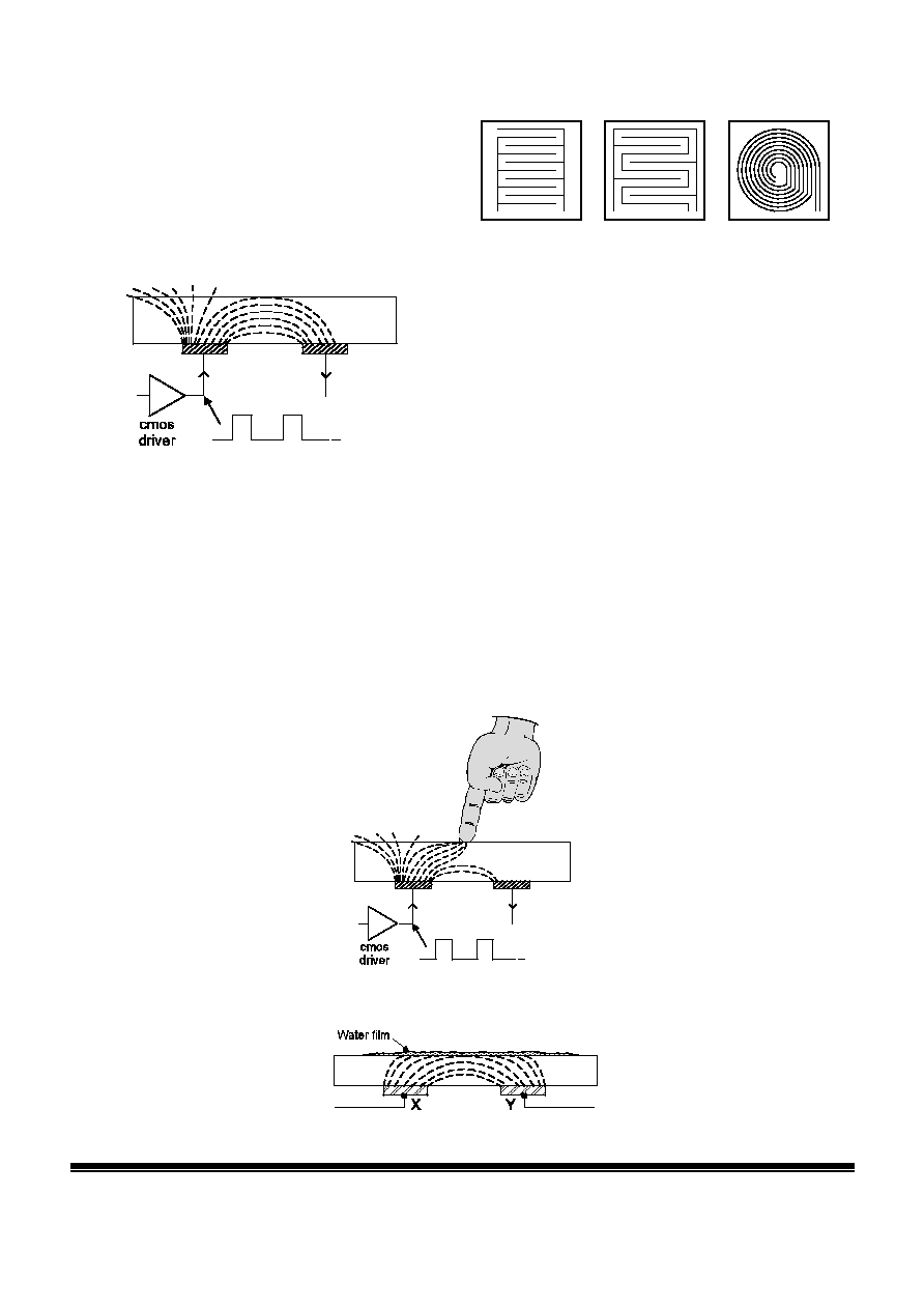
1.1 Field Flows
Figure 1-1 shows how charge is
transferred across an electrode set
to permeate the overlying panel
material; this charge flow exhibits a
high dQ/dt during the edge
transitions of the X drive pulse. The
charge driven by the X electrode is partly received onto the
corresponding Y electrode which is then processed. The part
uses 4 'X' edge-driven rows and 4 'Y' sense columns to sense
up to 16 keys.
The charge flows are absorbed by the touch of a human
finger (Figure 1-1) resulting in a decrease in coupling from X
to Y. Thus, received signals decrease or go negative with
respect to the reference level during a touch.
As shown in Figure 1-3, water films cause the coupled fields
to increase slightly, making them easy to distinguish from
touch.
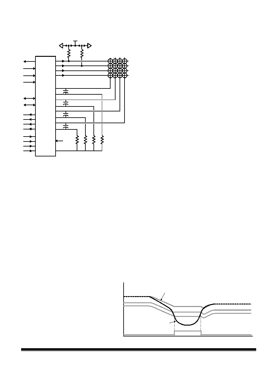
1.2 Circuit Overview
A basic circuit diagram is shown in Figure 1-5. The `X' drives
are sequentially pulsed in groupings of bursts. At the
intersection of each `X' and `Y' line in the matrix itself, where
a key is desired, should be an interdigitated electrode set
similar to those shown in Figure 1-4. See Quantum App Note
AN-KD01, or consult Quantum for application assistance.
The device uses fixed external capacitors to acquire charge
from the matrix during a burst of charge-transfer cycles; the
burst length can be varied to permit digitally variable key
signal gains. The charge is converted to digital using a
single-slope conversion process.
Burst mode operation permits the
use of a passive matrix, reduces RF
emissions, and provides excellent
response times.
Refer to Section 3 for more details
on circuit operation.
1.3 Communications
The device uses two variants of SPI
communications, Slave-only and
Master-Slave, a UART interface,
plus a parallel scan interface. Over
the serial interfaces are used a
command and data transfer
structure designed for high levels of
flexibility using minimal numbers of
bytes. For more information see
Sections 4 and 5.
The parallel scan port permits the
replacement of electromechanical
keypads that would be scanned by
a microcontroller; the scan interface
mimics an electromechanical
keyboard's response.
©Quantum Research Group Ltd.
l
Q
4
www.qprox.com QT60161B / R1.03
Figure 1-2 Field Flows When Touched
Figure 1-3 Fields With a Conductive Film
ov e rly in g pan el
X
element
Y
elem ent
Figure 1-4 Sample Electrode Geometries
PARALLEL LINES
SERPENTINE
SPIRAL
Figure 1-1 Field flow between X and Y elements
overly ing panel
X
element
Y
elem ent
2 Signal Processing
The device calibrates and processes signals using a number
of algorithms specifically designed to provide for high
survivability in the face of adverse environmental challenges.
The QT60161B provides a large number of processing
options which can be user-selected to implement very
flexible, robust keypanel solutions.
2.1 Negative Threshold
See also command ^A, page 21
The negative threshold value is established relative to a key's
signal reference value. The threshold is used to determine
key touch when crossed by a negative-going signal swing
after having been filtered by the detection integrator (Section
2.6). Larger absolute values of threshold desensitize keys
since the signal must travel farther in order to cross the
threshold level. Conversely, lower thresholds make keys
more sensitive.
As Cx and Cs drift, the reference point drift-compensates for
these changes at a user-settable rate (Section 2.4); the
threshold level is recomputed whenever the
reference point moves, and thus it also is drift
compensated.
The threshold is user-programmed on a per-key
basis using the setup process (Section 5).
2.2 Positive Threshold
See also command ^B, page 21
The positive threshold is used to provide a
mechanism for recalibration of the reference point
when a key's signal moves abruptly to the positive.
These transitions are described more fully in
Section 2.7.
The threshold is user-programmed using the setup process
described in Section 5 on a per-key basis.
2.3 Hysteresis
See also command ^C and ^D, page 21
Refer to Figure 1-6. The QT60161B employs programmable
hysteresis levels of 12.5%, 25%, or 50% of the delta between
the reference and threshold levels. There are different
hysteresis settings for positive and negative thresholds which
can be set by the user. The percentage refers to the distance
between the reference level and the threshold at which the
detection will drop out. A percentage of 12.5% is less
hysteresis than 25%, and the 12.5% hysteresis point is closer
to the threshold level than to the reference level.
The hysteresis levels are set for all keys only; it is not
possible to set the hysteresis differently from key to key on
either the positive or negative hysteresis levels.
2.4 Drift Compensation
See also commands ^H, ^I, page 22
Signal levels can drift because of changes in Cx and Cs over
time. It is crucial that such drift be compensated, else false
detections, non- detections, and sensitivity shifts will follow.
The QT60161B can compensate for drift using two setups, ^H
and ^I.
Drift compensation is performed by making the reference
level track the raw signal at a slow rate, but only while there is
no detection in effect. The rate of adjustment must be
performed slowly, otherwise legitimate detections could be
ignored. The devices drift compensate using a slew-rate
limited change to the reference level; the threshold and
hysteresis values are slaved to this reference.
When a finger is sensed, the signal falls since the human
body acts to absorb charge from the cross-coupling between
X and Y lines. An isolated, untouched foreign object (a coin,
or a water film) will cause the signal to rise very slightly due to
the enhanced coupling thus created. These effects are
contrary to the way most capacitive sensors operate.
Once a finger is sensed, the drift compensation mechanism
ceases since the signal is legitimately detecting an object.
Drift compensation only works when the key signal in
question has not crossed the negative threshold level
(Section 2.1).
The drift compensation mechanism can be made asymmetric
if desired; the drift-compensation can be made to occur in
one direction faster than it does in the other simply by setting
^H and ^I to different settings.
©Quantum Research Group Ltd.
l
Q
5
www.qprox.com QT60161B / R1.03
Figure 1-5 Circuit Block Diagram
X0
X1
X2
X3
Y0 Y1 Y2 Y3
KE
YM
A
T
RI
X
QT60161
SPI
to Host
X0
X1
X2
X3
CS0A
CS0B
Sample
CS0
Sample caps
CS1A
CS1B
CS2A
CS2B
CS3A
CS3B
CS1
CS2
CS3
UART
to Host
Sc
an I
n
p
u
t
Sca
n
O
u
t
p
ut
VREF
Reset
Wake /
Sync
Vcc
Opt A
Opt B
LED
Scope
Sync
Figure 1-6 Detection and Drift Compensation
Threshold
Signal
Hysteresis
Reference
Output

