RT9168/A
DS9168/A-03 May 2001
www.richtek-ic.com.tw
1
200mA/500mA Fixed Output Voltage LDO Regulator
General Description
The RT9168/A is a 200mA/500mA low dropout and
micropower regulator suitable for portable
applications. The output voltages range from 1.5V to
5.0V in 100mV increments and 2% accuracy. The
RT9168/A is designed for use with very low ESR
capacitors. The output remains stable even with a
1
µF ceramic output capacitor.
The RT9168/A uses an internal PMOS as the pass
device, which does not cause extra GND current in
heavy load and dropout conditions. The shutdown
mode of nearly zero operation current makes the IC
suitable for battery-powered devices. Other features
include current limiting and over temperature
protection. The SOP-8 and SOT-25 packages are
also available for larger power dissipation and
design flexibility.
Applications
Cellular Telephones
Laptop, Notebook, and Palmtop Computers
Battery-powered Equipment
Hand-held Equipment
Ordering Information
RT9168/A-
Features
Stable with Low-ESR Output Capacitor
Low Dropout Voltage (220mV at 200mA)
Low Operation Current - 80
µ
µ
µ
µA Typical
Shutdown Function
Low Temperature Coefficient
Current and Thermal Limiting
Custom Voltage Available
SOT-25 and SOP-8 Packages
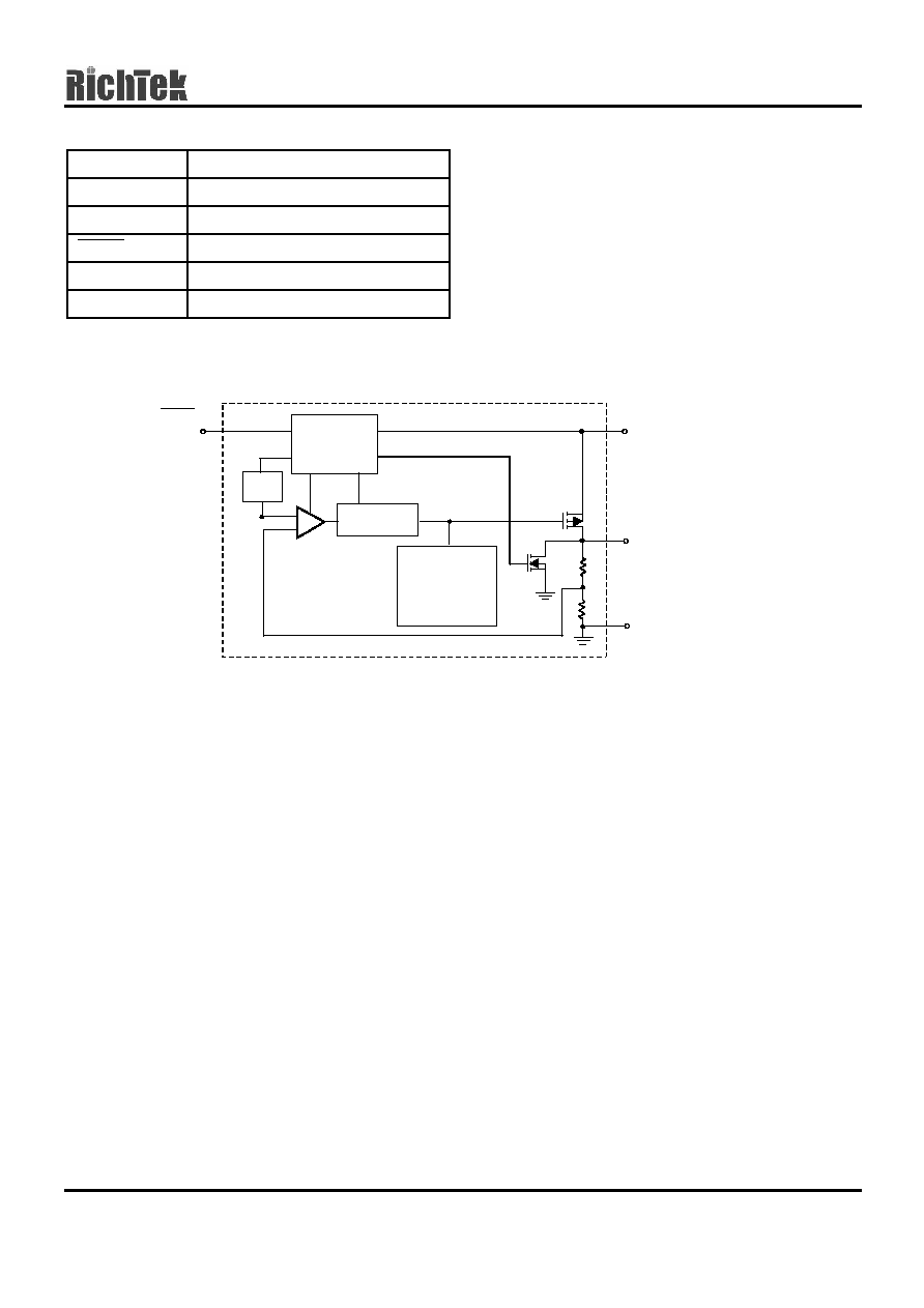
Pin Configurations
Part Number
Pin Configurations
RT9168/A-
CBR
(Plastic SOT-25)
TOP VIEW
1. OUT
2. GND
3. IN
4. SHDN
5. NC
RT9168/A-
CS
RT9168/A-
CSH
(Plastic SOP-8)
TOP VIEW
Typical Application Circuit
Package type
BR : SOT-25
S : SOP-8
SH : SOP-8, High shutdown
Operating temperature range
C: Commercial standard
Output voltage
15 : 1.5V
16 : 1.6V
:
:
49 : 4.9V
50 : 5.0V
500mA Output current
200mA Output current
5
4
3
2
1
OUT
GND
GND
NC
IN
GND
GND
SHDN/SHDN
1
2
3
4
8
7
6
5
RT9168
GND
IN
OUT
V
OUT
C
OUT
1
µF
V
IN
C
IN
1
µF
SHDN
NC
SHDN
RT9168/A
www.richtek-ic.com.tw
DS9168/A-03 May 2001
4
Absolute Maximum Ratings
Input Voltage
8V
Power Dissipation, P
D
@ T
A
= 25
∞C
SOT-25
0.25W
SOP-8
0.625W
Operating Junction Temperature Range
-40∞C to 125∞C
Storage Temperature Range
-65∞C to 150∞C
Package Thermal Resistance
SOT-25,
JA
250
∞C/W
SOP-8,
JA
160
∞C/W
Lead Temperature (Soldering, 5 sec.)
260
∞C
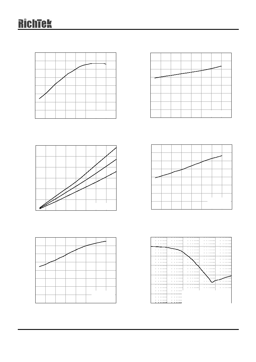
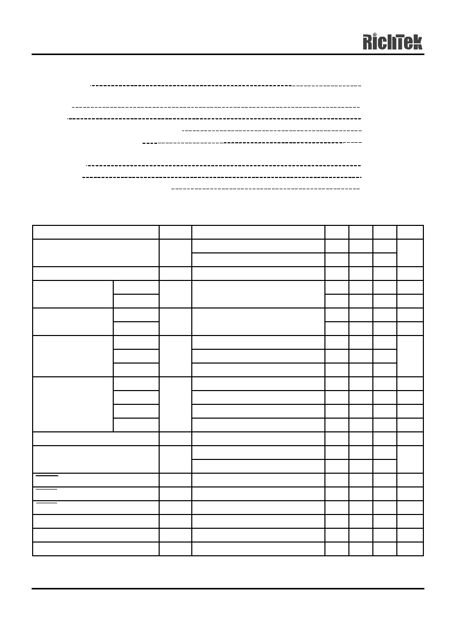
Electrical Characteristics
(V
IN
= 5.0V, C
IN
= 1
µF, C
OUT
= 1
µF, T
A
= 25
∞C, unless otherwise specified)
Parameter
Symbol
Test Conditions
Min
Typ
Max Units
2.9
--
7
Input Voltage Range
V
IN
I
L
= 50mA
2.7
--
7
V
Output Voltage Accuracy
V
OUT
I
L
= 1mA
-2
--
+2
%
RT9168
200
--
--
mA
Maximum Output
Current
RT9168A
I
MAX
500
--
--
mA
RT9168
--
300
--
mA
Current Limit
RT9168A
I
LIMIT
R
LOAD
= 1 Ohm
--
700
--
mA
RT9168/A
No Load
--
80
150
RT9168
I
OUT
= 200mA
--
90
150
GND Pin Current
RT9168A
I
G
I
OUT
= 500mA
--
90
150
µA
RT9168/A
I
OUT
= 1mA
--
1.1
5
mV
RT9168/A
I
OUT
= 50mA
--
55
100
mV
RT9168/A
I
OUT
= 200mA
--
220
300
mV
Dropout Voltage
(Note)
(V
OUT
(Nominal)
3.0V
Version)
RT9168A
V
DROP
I
OUT
= 500mA
--
600
750
mV
Line Regulation
V
LINE
V
IN
= (V
OUT
+0.15) to 7V, I
OUT
= 1mA
-0.2
--
+0.2
%/V
I
OUT
= 0mA to 200mA
--
0.01
0.04
Load Regulation
V
LOAD
I
OUT
= 0mA to 500mA
--
0.01
0.04
%/mA
SHDN, SHDN Input High Threshold V
IH
V
IN
= 3V to 5.5V
2.2
--
--
V
SHDN, SHDN Input Low Threshold V
IL
V
IN
= 3V to 5.5V
--
--
0.4
V
SHDN, SHDN Bias Current
I
SD
--
--
100
nA
Shutdown Supply Current
I
GSD
V
OUT
= 0V
--
0.01
1
µA
Thermal Shutdown Temperature
T
SD
--
155
--
∞C
Ripple Rejection
PSRR
F = 100Hz, C
BP
= 10nF, C
OUT
= 10
µF
--
58
--
dB
Notes: Dropout voltage definition: V
IN
- V
OUT
when V
OUT
is 50 mV below the value of V
OUT
at V
IN
= V
OUT
+ 0.5V