Äîêóìåíòàöèÿ è îïèñàíèÿ www.docs.chipfind.ru
Preliminary
RT9541
DS9541-05 August 2001
www.richtek-ic.com.tw
1
Li-Ion Battery Protector
General Description
The RT9541 Series are protection ICs for over-
charge/discharge of rechargeable one-cell Lithium-ion
(Li+) batteries by CMOS process.
The RT9541 Series can detect over-charge/discharge
of Li+ one-cell and excess load current and charge
current, further include a short circuit protector for
preventing large external short circuit current.
Each of these ICs is composed of four voltage
detectors, a reference unit, a hysteresis circuit, and a
bidirectional short circuit protector. Package of SOT-
26 is available.
Ordering Information
RT9541
Typical Application Circuit
Features
Low supply current
- Supply current: TYP. 2.0µµµµA
- Standby current (after detecting over-
discharge): Less than 0.2
µ
µ
µ
µA
High accuracy detector threshold
- Over-charge detector: ±±±±25mV
- Over-discharge detector: ±±±±2.5%
Built-in protection circuit
- Excess current trip/Short circuit protector in
both charging and discharging direction
Output delay of over-charge adjustable with
an external capacitor: 75mS at 0.01
µ
µ
µ
µF
Ultra small package: SOT26
Applications
Over-charge / Over-discharge Protection for Li+
One-cell Pack
High Precision Protectors for Cellular Phones or
Instruments Using Li+ One-cell Battery
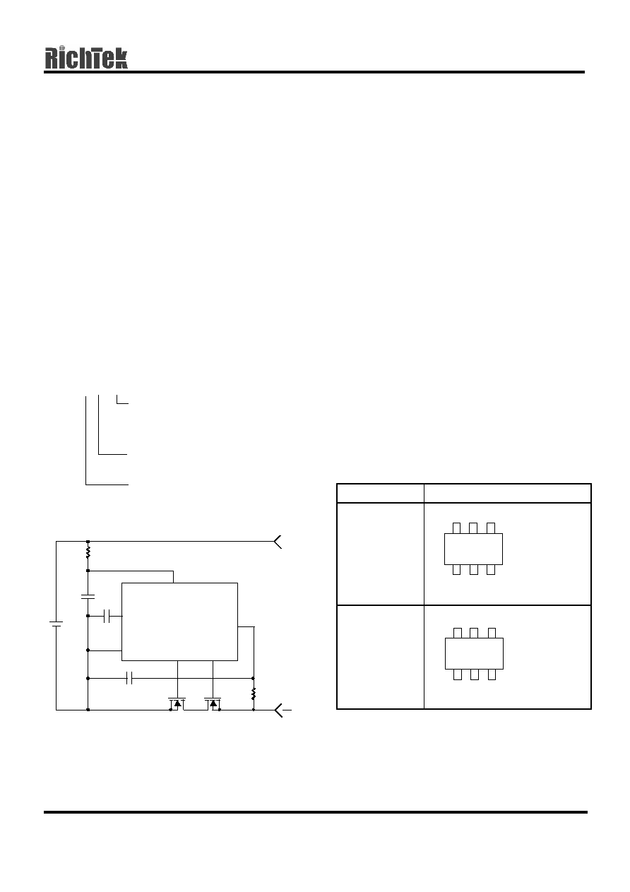
Pin Configurations
Part Number
Pin Configurations
RT9541 CE
(Plastic SOT-26)
TOP VIEW
1. COUT
2. CT
3. VSS
4. DOUT
5. VDD
6. V-
RT9541 CER
(Plastic SOT-26)
TOP VIEW
1. DOUT
2. V-
3. COUT
4. CT
5. VDD
6. VSS
6
4
3
2
1
5
6
4
3
2
1
5
Operating temperature range
C: Commercial standard
Package type
E : SOT-26 Type I
ER : SOT-26 Type II
See Table 1
RT9541
VDD
CT
VSS
DOUT
COUT
V-
+
R1
100
C1
0.1
µF
C3
0.01
µF
C2
0.1
µF
R2
1K
RT9541
Preliminary
www.richtek-ic.com.tw
DS9541-05 August 2001
2
Absolute Maximum Ratings
Allowable Battery Voltage
-0.3V ~ 7V
Input Voltage (V)
VDD-14V to VDD +0.3V
Input Voltage (CT)
VSS-0.3V to VDD +0.3V
Output Voltage (COUT)
VDD-14V to VDD +0.3V
Output Voltage (DOUT)
VSS-0.3V to VDD +0.3V
Power Dissipation, P
D
@ T
A
= 25
°C
SOT-26
0.25W
Package Thermal Resistance
SOT-26,
JA
250
°C/W
Operating Temperature Range
-20
°C ~ +85°C
Storage Temperature Range
-65
°C ~ +150°C
Electrical Characteristics
Parameter
Symbol
Test Conditions
Min
Typ
Max
Units
Operating Input Voltage
V
DD
Voltage defined as VDD-VSS
1
--
6
V
Charger Voltage
V
CHG
Voltage defined as VDD-V-
--
--
14
V
Minimum Operating Voltage for 0V
Charging
Voltage defined as VDD-V-
VDD-VSS = 0V
--
--
1
V
Accuracy of Over-charge
Threshold Voltage
V
OCHG
Detect rising edge of supply
voltage
-25
--
25
mV
Over-charge Threshold Hysteresis
0.1
0.15
0.2
V
Output Delay Time of Over-charge T
OCHG
C3 = 0.01
µF, VDD = 3.6V ~
4.3V
30
60
80
mS
Accuracy of Over-discharge
Threshold Voltage
V
ODISCHG
Detect falling edge of supply
voltage
-2.5
--
2.5
%
Output Delay Time of Over-
discharge
T
ODISCHG
VDD = 3.6V ~ 2.4V
10
15
20
mS
Excess Current Threshold Voltage
During Discharge
Detect rising edge of "V-" pin
voltage
0.15
0.17
0.19
V
Output Delay of Discharge Excess
Current
VDD = 3.0V
15
20
25
mS
Excess Current Threshold Voltage
During Charge
Detect falling edge of "V-" pin
voltage
-0.19
-0.17
-0.15
V
Output Delay of Charge Excess
Current
15
20
25
mS
Short Detection Voltage During
Discharge
VDD = 3.0V
VDD-1.1 VDD-0.8 VDD-0.5
V
Output Delay of Discharge Short
Circuit
T
SHORT
VDD = 3.0V
--
5
50
µS
Reset Resistance for Excess
Current Protection
R
SHORT
VDD = 3.6V, V- = 1.0V
25
50
75
k
Supply Current
I
DD
VDD = 3.9V, V- = 0V
--
2.0
5.0
µA
Standby Current
I
STANDBY
VDD = 2.0V
--
0.1
0.5
µA
Preliminary
RT9541
DS9541-05 August 2001
www.richtek-ic.com.tw
3
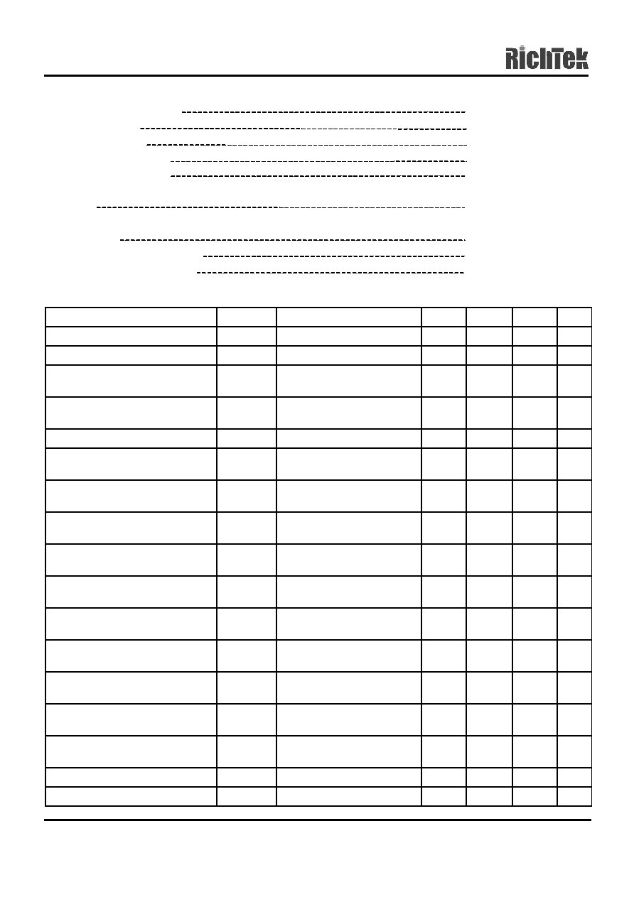
Table 1
Part Number
Over
Charge
Over
Discharge
Excess
Current
RT9541ACE (R)
4.25V
2.3V
170mV
RT9541BCE (R)
4.25V
2.4V
170mV
RT9541CCE (R)
4.25V
2.5V
170mV
RT9541DCE (R)
4.25V
2.6V
170mV
RT9541ECE (R)
4.25V
2.7V
170mV
RT9541FCE (R)
4.25V
2.8V
170mV
RT9541GCE (R)
4.30V
2.3V
170mV
RT9541HCE (R)
4.30V
2.4V
170mV
RT9541ICE (R)
4.30V
2.5V
170mV
RT9541JCE (R)
4.30V
2.6V
170mV
Part Number
Over
Charge
Over
Discharge
Excess
Current
RT9541KCE (R)
4.30V
2.7V
170mV
RT9541LCE (R)
4.30V
2.8V
170mV
RT9541MCE (R)
4.35V
2.3V
170mV
RT9541NCE (R)
4.35V
2.4V
170mV
RT9541OCE (R)
4.35V
2.5V
170mV
RT9541PCE (R)
4.35V
2.6V
170mV
RT9541QCE (R)
4.35V
2.7V
170mV
RT9541RCE (R)
4.35V
2.8V
170mV
RT9541SCE (R)
4.35V
2.9V
170mV
RT9541TCE (R)
4.25V
2.9V
170mV
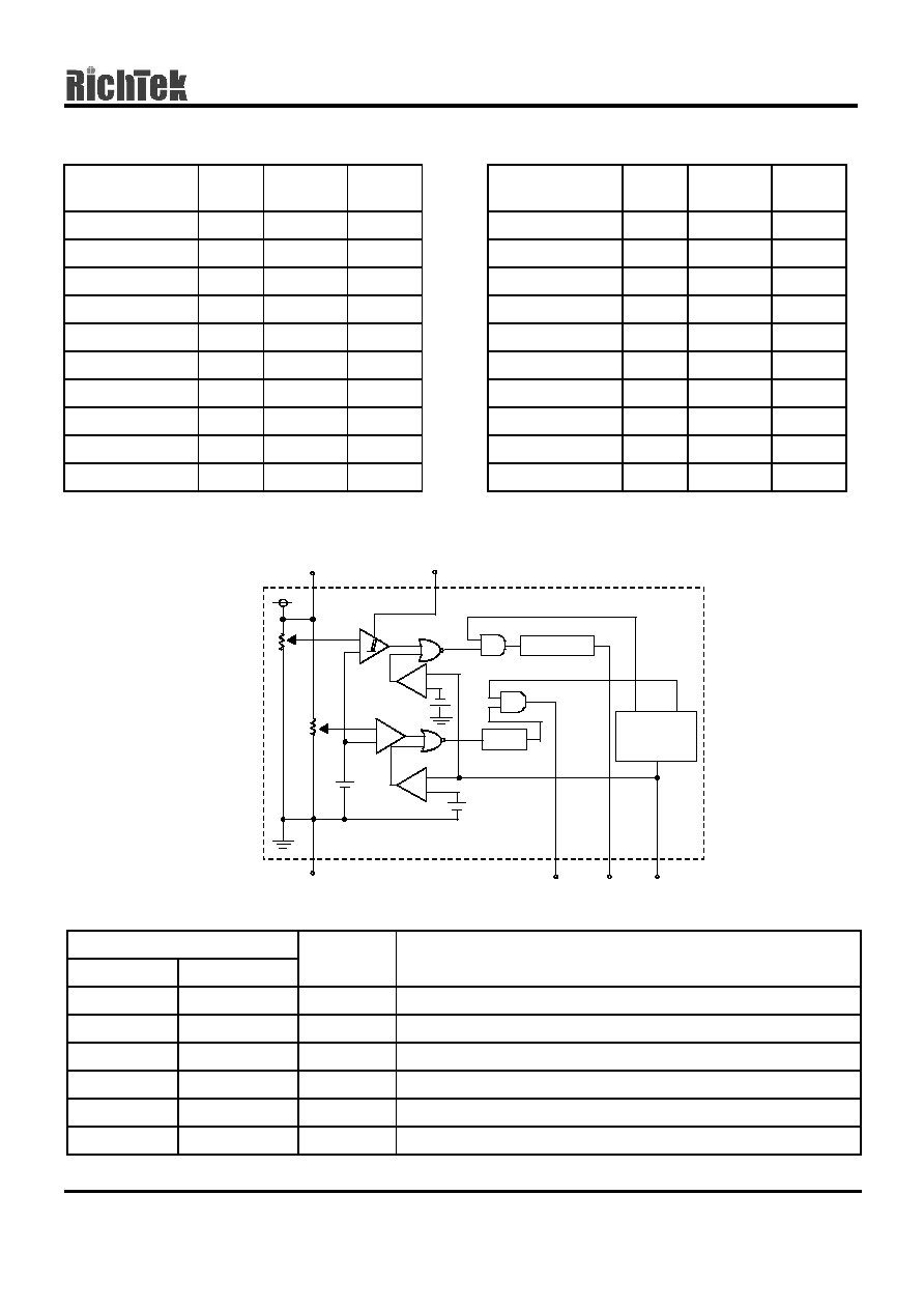
Function Block Diagram
Pin Description
Pin Number
RT9541- CE RT9541- CER
Pin Name
Pin Function
1
3
COUT
Output of Over-charge Detection, CMOS Output
2
4
CT
Pin for External Capacitor Setting Output Delay of VD1
3
6
VSS
Ground
4
1
DOUT
Output of Over-discharge Detection, CMOS Output
5
5
VDD
Power Supply, through a Resistor (R1)
6
2
V-
Pin for Charger Negative Input, through a Resistor (R2)
Short
Circuit
Detector
Level Shift
Delay
VDD
CT
VD1
VD4
VD2
VD3
VSS
DOUT COUT
V-
+
_
+
_
+
_
+
_

RT9541
Preliminary
www.richtek-ic.com.tw
DS9541-05 August 2001
4
Applications Information
(1) Operation Description
Refering to the "Function Block Diagram", when
charging voltage crosses the detector threshold from
a low value to a value higher than VDET1, the output
of COUT pin, the output of over-charge detector/VD1,
swiches to low level,..charger's negative pin level.
After detecting over-charge the VD1 can be reset and
the output of COUT pin becomes "H" when the VDD
voltage is coming down to a level lower than "VDET1
VHYS1", or when a charger is disconnected from
the battery pack.
The output of DOUT pin, the output of over-discharge
detector/VD2, switches to "L" after internally fixed
delay time passed, when discharging voltage crosses
the detector threshold from a high value to a value
lower than VDET2. An excess load current can be
sensed and cut off after internally fixed delay time
passsed through the built in excess current detector,
VD3, with DOUT being enabled to low level. Once
after detecting excess current, the VD3 is released
and DOUT level switches to "H" by detaching a
battery pack from a load system.
Futher, short circuit protector makes DOUT level to
"L" immediately with external short circuit current and
removing external short circuit leads DOUT level to
"H".
The excess charging current is also monitored, and
the charging path will be cut off (by turn low COUT)
after excess charging current was detected lasting a
internally fixed delay time. The charging path will be
re-started (by turn high COUT) after another
internally fixed delay. If the excess charging current is
still there, the same process will be repeated and
cause the charging path toggling on and off with a
12.5% on duty. Such a protection function reduces
the average charging current to 12.5% of original
value when excess charging current detected.
The short circuit protection function in charging
direction was also provided. When COUT high and
the "V-" pin voltage 5V lower than VSS pin, the
RT9541 will turn low COUT with a fixed delay. The
COUT will go high after the short circuit condition
was removed.
After detecting over-discharge, supply current will be
kept extremely low by halting some internal circuits
operation. The output delay of over-charge detectors
can be set by connecting an external capacitor.
Output type of COUT and DOUT are CMOS.
(2) Component Selection Guide:
Referring to "Typical Application Circuit", R1 and
C1 will stabilize a supply voltage to the RT9541. A
recommended R1 value is less than 1k. A larger
value of R1 leads higher detection voltage, makes
some errors, because of shoot through current
flowed in the RT9541.
R2 and C2 will stabilize a V- pin voltage. The
resetting from over-discharge with connecting
charger possibly be disabled by larger value of R2.
Recommended value is less than 1k. And
recommended C2 value is less than 1
µF.
R1 and R2 can operate as a current limiter against
setting cell reverse direction or for applying excess
charging voltage to the RT9541. While smaller R1
and R2 may cause an over power dissipation rating
of the RT9541 and a total of "R1+R2" should be
more than 1k.
Preliminary
RT9541
DS9541-05 August 2001
www.richtek-ic.com.tw
5
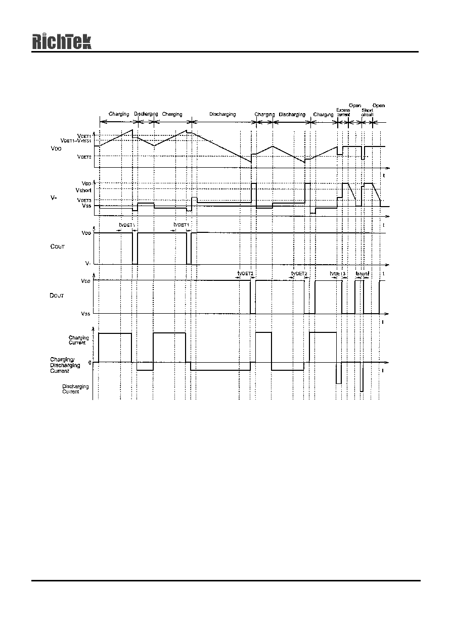
Timing Diagram
RT9541- CE/CER
RT9541
Preliminary
www.richtek-ic.com.tw
DS9541-05 August 2001
6
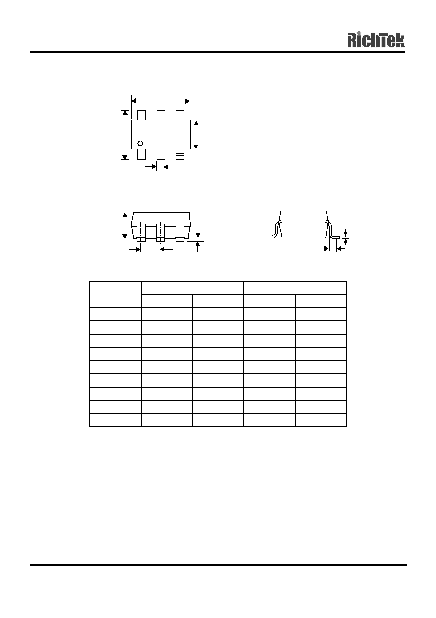
Package Information
Dimensions In Millimeters
Dimensions In Inches
Symbol
Min
Max
Min
Max
A
0.889
1.295
0.035
0.051
A1
--
0.152
--
0.006
B
1.397
1.803
0.055
0.071
b
0.356
0.559
0.014
0.022
C
2.591
2.997
0.102
0.118
D
2.692
3.099
0.106
0.122
e
0.838
1.041
0.033
0.041
H
0.102
0.254
0.004
0.010
L
0.356
0.610
0.014
0.024
b
B
C
D
L
H
A1
e
A

Preliminary
RT9541
DS9541-05 August 2001
www.richtek-ic.com.tw
7

RT9541
Preliminary
www.richtek-ic.com.tw
DS9541-05 August 2001
8
RICHTEK TECHNOLOGY CORP.
Headquarter
6F, No. 35, Hsintai Road, Chupei City
Hsinchu, Taiwan, R.O.C.
Tel: (8863)5510047 Fax: (8863)5537749
RICHTEK TECHNOLOGY CORP.
Taipei Office (Marketing)
8F-1, No. 137, Lane 235, Paochiao Road, Hsintien City
Taipei County, Taiwan, R.O.C.
Tel: (8862)89191466 Fax: (8862)89191465
Email: marketing@richtek-ic.com.tw
Document Outline