UTC339
LINEAR INTEGRATED CIRCUIT
YOUW ANG ELECTRONICS CO.LTD
1
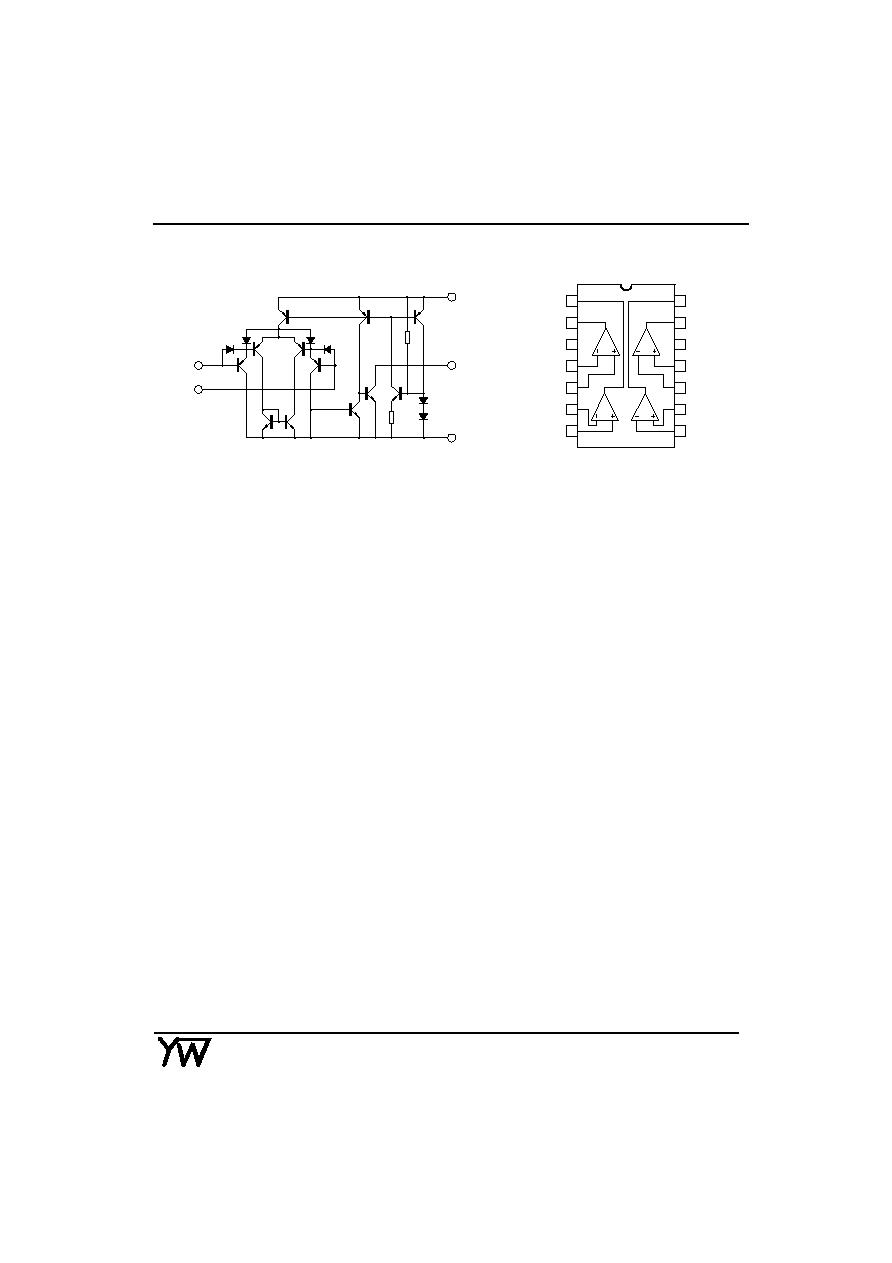
QUAD DIFFERENTIAL
COMPARATOR
DESCRIPTION
The UTC339 consists of four independent voltage
comparators designed specifically to operate from a
single power supply over a wide voltage range.
FEATURES
*Single or dual supply operation
*Wide operating supply range(Vcc=2V~36V)
*Input common-mode voltage includes ground
*Low supply current drain ICC=0.8mA(Typical)
*Open collector outputs for wired and connection
*Low input bias current Ibias=25nA(Typical)
*Low output saturation voltage
*Output compatible with TTL ,DTL, and CMOS logic
system
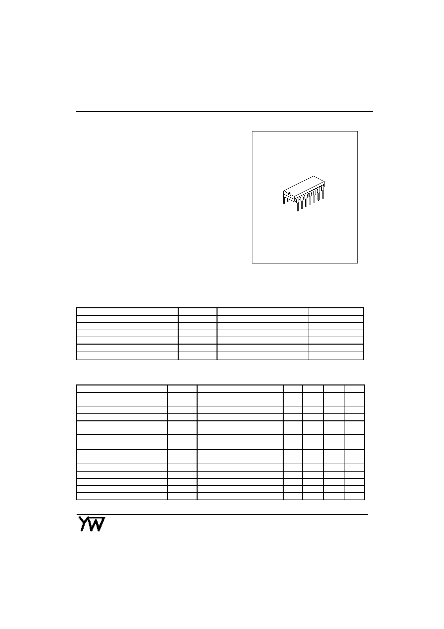
DIP-14
ABSOLUTE MAXIMUM RATINGS
(Ta=25
°
C
)
Characteristic
Symbol
Value
Unit
Supply Voltage
Vcc
±
18 OR 36
V
Differential input voltage
VIDiff)
36
V
Input Voltage
VI
-0.3~36V
V
Power Dissipation
Pd
570
mW
Operating Temperature
Topr
0 to +70
°
C
Storage Temperature
Tstg
-65 to 150
°
C
ELECTRICAL CHARACTERISTICS
(Vcc=5.0V, Ta=25
k
,All voltage referenced to GND unless otherwise specified)
Characteristic
Symbol
Test Condition
Min
Typ.
Max
Unit
Input offset voltage
V
IO
V
CM
=0 to Vcc-1.5
Vo(p)=1.4V,Rs=0
±
1.5
±
5.0
mV
Input offset current
I
IO
±
2.3
±
50
nA
Input Bias current
Ib
57
250
nA
Input Common-mode voltage
range
V
I(R)
0
Vcc-
1.5
V
Supply Current
Icc
R
L
=
1.1
2.0
mA
Large signal Voltage Gain
G
V
Vcc=15V,R
L
>15k
50
200
V/mV
Large signal response time
tres
Vi=TTL logic wing
Vref=1.4V,V
RL
=5V,R
L
=5.1k
350
ns
Response time
tres
V
RL
=5V,R
L
=5.1k
1400
ns
Output sink current
Isink
Vi(-)>1V,Vi(+)=0V,Vo(p)<1.5V
6
18
mA
Output saturation voltage
Vsat
Vi(-)>1V,Vi(+)=0V,Isink=4mA
140
400
mV
output leakage current
Ileakage
VI(+)=1V,VI(-)=0
20
40
mA
Differential input voltage
VI(diff)
36
V
UTC339
LINEAR INTEGRATED CIRCUIT
YOUW ANG ELECTRONICS CO.LTD
3
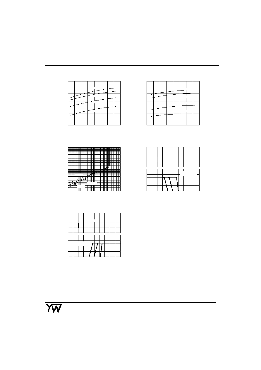
TYPICAL CHARACTERISTICS PERFORMANCE
0
5
10
15
20
25
30
35
40
0.2
0.4
0.6
0.8
1.0
1.2
1.4
1.6
1.8
2.0
2.2
Ta=-25
k
Ta=-40
k
Ta=25
k
Ta=70
k
RL=
Fig.1 supply current
s
uppl
y
c
u
r
r
ent
(
m
A)
Supply voltage (V)
0
5
10
15
20
25
30
35
40
10
20
30
40
50
60
70
80
90
100
110
Ta=-25
k
Ta=-40
k
Ta=25
k
Ta=70
k
Vcm=0V
DC
Rcm=1G
Fig.2 Input current
Input
c
u
r
r
ent
(
m
A)
Supply current (V)
(
µ
s)
0
0.4
0.8
1.2
1.6
0
2.0
4.0
6.0
-100
0
output
v
o
ltage
(V)
input
v
o
ltage
(m
V)
Fig.4 Reponse time for various input overdrive
negative transition
Ta=25
k
input overdrive
50mV
20mV
5.0mV
10
-3
1
10
10
2
10
-2
10
-2
-1
10
-1
10
1
10
1
1
Fig.3 Output saturation voltage
s
a
tur
a
tion
v
o
ltage(
V
)
Output sink current (mA)
Ta=85
k
Ta=25
k
Ta=-40
k
0
0.4
0.8
1.2
1.6
(
µ
s)
0
2.0
4.0
6.0
O
u
tput
v
o
ltage
(
V
)
I
nput
v
o
ltage
(
m
V
)
0
100
50mV
20mV 5.0mV
Input overdrive
Ta=25
k
Fig.4 Reponse time for various input overdrive
negative transition
Fig.4 Reponse time for various input overdrive
positive transition
UTC339
LINEAR INTEGRATED CIRCUIT
YOUW ANG ELECTRONICS CO.LTD
4
Time (
µ
s)
Frequency (Hz)
6
10
4
10
10
3
5
10
0
5
10
15
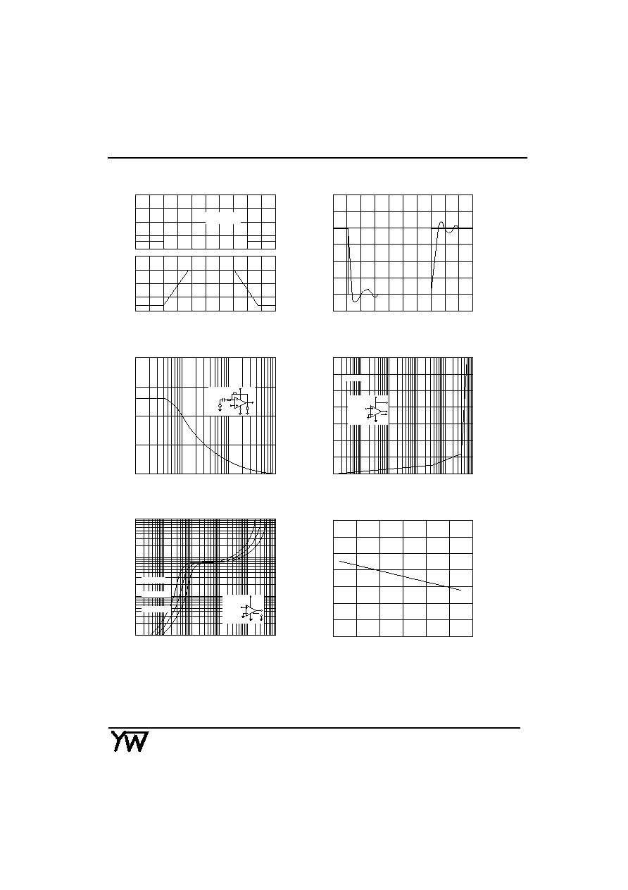
Fig.9 Large signal Frequency Response
O
u
t
put
sw
i
n
g
(
Vp-
p
)
100k
2k
1k
Vi
+15V
+7V
Vcc
Vcc/2
Io
Vo
Vcc=+5V
Vcc=+15V
Vcc=+30V
10
-3
10
-2
10
-1
1
10
2
10
10
-1
1
10
Fig.11 Output Characteristics Current sinking
O
u
tput
Vol
t
age
(
V
)
Output Sink Current (mA)
10
-1
10
-2
10
-3
10
2
10
1
1
2
3
4
5
6
7
8
Vcc
Vcc/2
Io
Vo
Ta=25
k
Fig.10 Output Characteristics
current sourcing
O
u
tput
r
e
ffer
enc
e
V
c
c
(
V
)
Output Source current (mA)
Fig.8 voltage Follower pulse response
(small signal)
O
u
tput
v
o
l
t
gae
(
V
)
0
1
2
3
4
5
6
7
8
9
275
300
350
400
450
Input
Vol
t
age
(
V
)
O
u
tput
Vol
t
age
(
V
)
Time (
µ
s)
RL=2k
Vcc=15V
0
1
2
3
2
3
1
0
0
10
20
30
40
50
Fig.7
-50
-25
0
25
50
75
100
0
20
40
60
Temperature ( )
k
O
u
tput
Cur
r
ent
(
m
A)
Fig.12 Current Limiting