UTC8227
LINEAR INTEGRATED CIRCUIT
YOUW ANG ELECTRONICS CO.LTD
1
LOW FREQUENCY POWER
AMPLIFIER
DESCRIPTION
The UTC8227 is the audio power amplifier with built-in
two channel developed for portable radio cassette tape
recorder with power ON/OFF switch.
FEATURES
*Wide operating supply voltage: Vcc=5~12V
*Low quiescent supply current
(Icc=21mA,typical,at Vcc=9V ,Vi=0)
*Output power
Po=2.50W/CH at Vcc=9V,R
L
=4ohm ,f=1kHz,Thd=10%
*Soft Clip
*Built-in Thermal shut-down protection circuit
*Stand-by Switch
HDIP-12
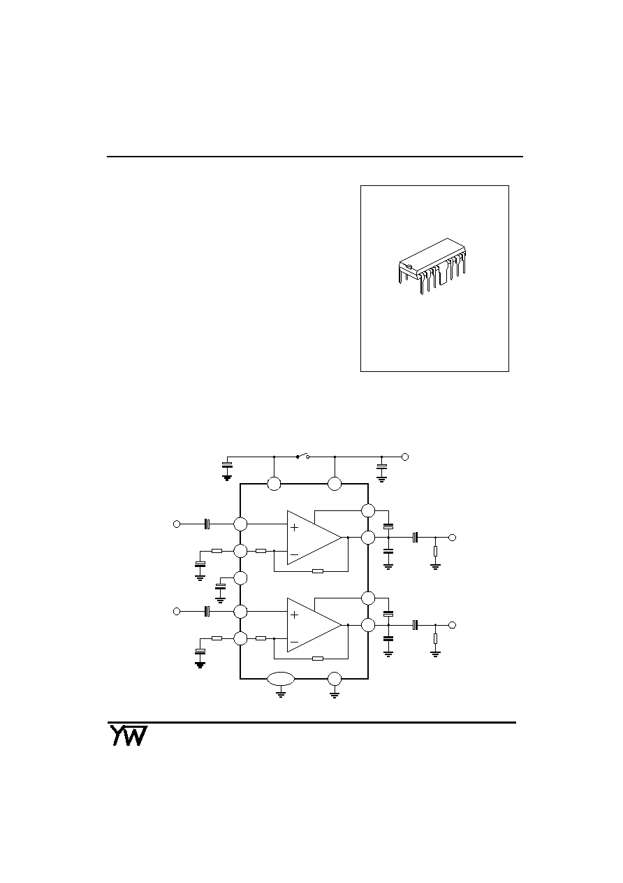
TEST CIRCUIT
30k
30k
45
45
Input 1
NF1
Ripple
Input 2
NF2
Boot
strap 1
Output 1
Boot
strap 2
Output 2
RL
RL
120
120
47
�
F
47
�
F
47
�
F
100
�
F
100
�
F
0.015
�
F
0
.015
�
F
1000
�
F
1000
�
F
100
�
F
1000
�
F
Vcc1
Vcc2
SW1
Power
GND
Pre
GND
6
5
7
8
9
TAB
4
3
2
10
11
1
12

UTC8227
LINEAR INTEGRATED CIRCUIT
YOUW ANG ELECTRONICS CO.LTD
2
ABSOLUTE MAXIMUM RATINGS
(Ta=25
�
C)
Characteristic
Symbol
Value
Unit
Supply Voltage
Vcc
20
V
Output Current
Io
2.5
A
Power Dissipation(note)
Pd
4
W
Operating Temperature
Topr
-20 ~ +75
�
C
Storage Temperature
Tstg
-55 ~ +150
�
C
Note: Value for mounting on PC board
ELECTRICAL CHARACTERISTICS
(Ta=25
�
C,Vcc=9V,RL=4
,Rg=600
,f=1kHz,unless otherwise specified)
Characteristic
Symbol
Test Conditions
Min
Typ
Max Units
Quiescent current
Icc
Vi=0
21
45
mA
THD=10%,RL=4
2.0
2.5
W
Output Power
Po
THD=10%,RL=3
3.0
W
Total Harmonic Distortion
THD
Po=0.4W/CH
0.2
1.0
%
Gv1
R
f
=120
,Vout=0.775Vrms
43
45
47
dB
Voltage Gain
Gv2
R
f
=0,Vout=0.775Vrms
56.5
Input Impedance
Rin
30
Output Noise Voltage
Vno
Rg=10k
,BW=20Hz~20kHz
0.3
1.0
mVrms
Ripple Rejection Ratio
R.R
Rg=600
fripple=100Hz
52
dB
Cross Talk
C.T
Rg=600
,Vout=0, f=1kHz
50
dB
Input Offset Voltage
V7,8
30
60
mV
Standby Current
Sw1:OFF
1
�
A

UTC8227
LINEAR INTEGRATED CIRCUIT
YOUW ANG ELECTRONICS CO.LTD
3
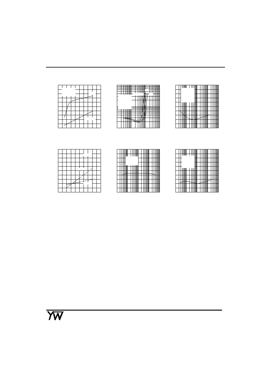
TYPICAL PERFORMANCE CHARACTERISTICS
0
3
6
9
12
15
0
3
6
9
12
15
Vcc1=12V
Vin=0
Ta=25
k
ICCQ, V2,V10 vs. VCC1
Supply Voltage , Vcc2 (V)
Qui
e
s
c
ent
c
u
rrent
(m
A
)
0
3
6
9
12
15
Out
put
V
o
l
t
age
(V
)
I
CCQ
V
10
,V
2,
Output Power (W)
T
o
t
a
l
H
arm
oni
c
D
i
s
t
o
rt
i
o
n
(
%
)
0.1
1
10
0.01
0.1
1
10
THD vs Output Power
Vcc2=5V
6V
9V
Vcc1=9V
RL=4
f=1kHz
RNF=120
Ta=25
k
ICCQ, DC Vout vs. Supply Voltage
0
5
10
15
20
25
Supply Voltage , Vcc2 (V)
0
20
40
60
80
100
Qui
e
s
c
ent
c
u
rrent
(m
A
)
Vin=0
Vout
I
CCQ
0
4
8
12
16
20
Out
put
V
o
l
t
age
(V
)
Voltage Gain vs. Frequency
Frequency ( Hz)
Vo
lta
g
e
G
a
in
(
d
B)
10
1
10
2
10
3
10
4
10
5
0
20
40
60
80
Vcc=9V
R
L
=4
R
NF
=120
Frequency ( Hz)
10
1
10
2
10
3
10
4
10
5
Vo
lta
g
e
G
a
in
(
d
B)
-80
-60
-40
-20
0
Ripple Rejection vs. frequency
Vcc=9V
R
L
=4
R
NF
=120
Rg=620
Frequency ( Hz)
10
1
10
2
10
3
10
4
10
5
C
r
os
s
T
al
k
(
dB
)
-80
-60
-40
-20
0
Cross Talk vs. Frequency
Vcc=9V
R
L
=4
R
NF
=120
Rg=620
Vout=0dBm
APPLICATION INFORMATION
1.Input Voltage
When the excessive signal is input, turning-up is produced in the clip waveform. The turning-up point is
Vin=300mVrms(Typical) at Vcc=9V,RL=4
f=1kHz. Enough care must be taken for this phenomenon.
2.Power ON/OFF
There is power ON/OFF switch at pin 1. However output power is changed by pin 1 supply voltage when
pin1 supply voltage is not same pin 12 supply voltage, after referring to attached date, select pin 1 supply voltage.
3.Voltage Gain
The voltage gain can be changed by the external negative feedback resistor. When Rf=0, the Gain is equal
to 56.5dB.When Rf=120
the Gain is equal to 45dB.


