3/7/2006
W65C51S
Asynchronous Communications
Interface Adapter (ACIA)

2
WDC reserves the right to make changes at any time without notice in order to improve design and
supply the best possible product. Information contained herein is provided gratuitously and without
liability, to any user. Reasonable efforts have been made to verify the accuracy of the information
but no guarantee whatsoever is given as to the accuracy or as to its applicability to particular uses.
In every instance, it must be the responsibility of the user to determine the suitability of the
products for each application. WDC products are not authorized for use as critical components in
life support devices or systems. Nothing contained herein shall be construed as a recommendation
to use any product in violation of existing patents or other rights of third parties. The sale of any
WDC product is subject to all WDC Terms and Conditions of Sales and Sales Policies, copies of
which are available upon request.
Copyright 1981 2006 by The Western Design Center, Inc. All rights reserved, including the right
of reproduction, in whole, or in part, in any form.

3
1
28
27
26
2
3
4
24
15
12
16
18
14
13
17
22
21
20
19
25
23
8
6
7
5
9
10
11
W65C51S
RESB
CS1B
VSS
CS0
IRQB
RWB
PHI2
DB6
DB5
DB4
DB7
DB2
DB1
DB3
DCDB
DSRB
RS1
VDD
DB0
RS0
RxD
DTRB
TxD
XTLO
XTLI
RTSB
CTSB
RxC
DESCRIPTION
The WDC CMOS W65C51S Asynchronous Communications
Interface Adapter (ACIA) provides an easily implemented,
program controlled interface between 8-bit microprocessor
based systems and serial communication data sets and
modems.
The ACIA has an internal baud rate generator. This feature
eliminates the need for multiple component support circuits,
a crystal being the only other part required. The Transmitter
baud rate can be selected under program control to be either 1
of 15 different rates from 50 to 19,200 baud, or at 1/16 times
an external clock rate. The Receiver baud rate may be
selected under program control to be either the Transmitter
rate or at 1/16 times the external clock rate. The ACIA has
programmable word lengths of 5, 6, 7 or 8 bits; even, odd or
no parity; 1, 1� or 2 bit stops.
The ACIA is designed for maximum-programmed control
from the microprocessor (MPU) to simplify hardware
implementation. Three separate registers permit the MPU to
easily select the W65C51S operating modes and data
checking parameters and determine operational status.
The Command Register controls parity, receiver echo mode,
transmitter interrupt control, the state of the RTSB line,
receiver interrupt control and the state of the DTRB line.
The Control Register controls the number of stop bits, word
length, receiver clock source and baud rate.
The Status Register indicates the states of the IRQB, DSRB,
and DCDB lines, Transmitter and Receiver Data Registers
and Overrun, Framing and Parity Error conditions.
The Transmitter and Receiver Data Registers are used for
temporary data storage by the ACIA Transmit and Receiver
circuits.
Figure 1 W65C51S ACIA
28 Pin PLCC
FEATURES
� Low power CMOS N-well silicon gate
technology
� Replacement for CMD / GTE Harris / MOS
Technology / GE/RCA / Synertek / Motorola /
Rockwell R6551, 65SC51, 65C51, 6551,
CPD65C51, 6551, 6850
� Full duplex operation with buffered receiver
and transmitter
� Data set/modem control functions
� Internal baud rate generator with 15
programmable baud rates (50 to 19,200)
� Program-selectable internally or externally
controlled receiver rate
� Programmable word lengths, number of stop
bits and parity bit generation and detection
� Programmable interrupt control
� Program reset
� Program-selectable serial echo mode
� Two chip selects
� 2 or 4 MHz operation
� 5.0 VDC � 5% supply requirements
� 28 pin plastic DIP package
� 28 pin PLCC package
� Full TTL compatibility
� Compatible with 65xx and 68xx
microprocessors
Figure 2 W65C51S ACIA 28 Pin DIP
1
28
27
26
2
3
4
24
15
12
16
18
14
13
17
22
21
20
19
25
23
8
6
7
5
9
10
11
W65C51S
RE
S
B
CS
1
B
VS
S
CS
0
IR
Q
B
RW
B
PH
I2
DB6
DB5
DB4
DB7
DB2
D1
DB3
DCD
B
DS
RB
RS
1
VD
D
D0
RS
0
Rx
D
DTRB
TxD
XTLO
XTLI
RTSB
CTSB
RxC

4
Figure 3 ACIA Internal Organization
FUNCTIONAL DESCRIPTION
A block diagram of the ACIA is presented in Figure 2
followed by a description of each functional element of the
device
.
DATA BUS BUFFERS
The Data Bus Buffer interfaces the system data lines to the
internal data bus. The Data Bus Buffer is bi-directional.
When the RWB line is high and the chip is selected, the Data
Bus Buffer passes the data from the system data lines to the
ACIA internal data bus. When the RWB line is low and the
chip is selected, the Data Bus Buffer writes the data from the
internal data bus to the system data bus.
INTERRUPT LOGIC
The Interrupt Logic will cause the IRQB line to the
microprocessor to go low when conditions are met that
require the attention of the microprocessor. The conditions
which can cause an interrupt will set bit 7 and the appropriate
bit of bits 3 through 6 in the Status Register, if enabled. Bits
5 and 6 correspond to the Data Carrier Detect (DCDB) logic
and the Data Set Ready (DSRB) logic. Bits 3 and 4
correspond to the Receiver Data Register full and the
Transmitter Data Register empty conditions. These
conditions can cause an interrupt request if enabled by the
Command Register.
I/O CONTROL
The I/O Control Logic controls the selection of internal
registers in preparation for a data transfer on the internal data
bus and the direction of the transfer to or from the register.
The registers are selected by the Register Select (RS1, RS0)
and Read/Write (RWB) lines as described later in Table 1.
TIMING AND CONTROL
The Timing and Control logic controls the timing of data
transfers on the internal data bus and the registers, the Data
Bus Buffer and the microprocessor data bus and hardware
reset features.
Timing is controlled by the system PHI2 clock input. The
chip will perform data transfers to or from the microcomputer
data bus during the PHI2 high period when selected.
The Timing and Control Logic will initialize all registers
when the Reset (RESB) line goes low. See the individual
register description for the state of the registers following a
hardware reset.
TRANSMITTER AND RECEIVER DATA
REGISTERS
These registers are used as temporary data storage for the
ACIA Transmit and Receive Circuits. Both the Transmitter
and Receiver are selected by a Register Select 0 (RS0) and
Register Select 1 (RS1) low condition. The Read/Write
(RWB) line determines which actually uses the internal data
bus; the Transmitter Data Register is write only and the
Receiver Data Register is read only.
Bit 0 is the first bit to be transmitted from the Transmitter
Data Register (least significant bit first). The higher order
bits follow in order. Unused bits in this register are "don't
care".
The Receiver Data Register holds the first received data bit in
bit 0 (least significant bit first). Unused high-order bits are
"0". Parity bits are not contained in the Receiver Data
Register. They are stripped off after being used for parity
checking.

5
STATUS REGISTER
The Status Register indicates the state of interrupt conditions
and other non-interrupt status lines. The interrupt conditions
are the Data Set Ready, Data Carrier Detect, Transmitter
Data Register Empty and Receiver Data Register Full as
reported in bits 6 through 3, respectively. If any of these bits
are set the interrupt (IRQ) indicator (bit 7) is also set.
Overrun, Framing Error and Parity Error are also reported
(bits 2 through 0 respectively).
Bit 7
Interrupt (IRQ)
0 No
Interrupt
1 Interrupt
has
occurred
Bit 6
Data Set Ready (DSRB)
0
DSR low (ready)
1
DSR high (not ready)
Bit 5
Data Carrier Detect (DCDB)
0
DCD low (detected)
1
DCD high (not detected)
Bit 4
Transmitter Data Register Empty
0 Not
Empty
1 Empty
Bit 3
Receiver Data Register Full
0 Not
full
1 Full
Bit 2
Overrun*
0 No
overrun
1
Overrun has occurred
Bit 1
Framing Error*
0
No framing error
1
Framing error detected
Bit 0
Parity Error*
0
No parity error
1
Parity error detected
*No interrupt occurrs for these conditions
Reset Initialization
7 6 5 4 3 2 1 0
0 - - 1 0 0 0 0 Hardware
reset
- - - - - 0 - - Program
reset
Parity error (Bit 0) Framing Error (Bit 1) and Overrun
(Bit 2)
None of these bits causes a processor interrupt to occur but,
they are normally checked at the time the Receiver Data
Register is read so that the validity of the data can be
verified. These bits are self clearing (i.e., they are
automatically cleared after a read of the Receiver Data
Register).
Receiver Data Register Full (Bit 3)
This bit goes to a 1 when the ACIA transfers data from the
Receiver Shift Register to the Receiver Data Register and
goes to a 0 (is cleared) when the processor reads the Receiver
Data Register.
Transmitter Data Register Empty (Bit 4)
This bit goes to a 1 when the ACIA transfers data from the
Transmitter Data Register to the Transmitter Shift Register
and goes to a 0 (is cleared) when the processor writes new
data onto the Transmitter Data Register.
Data Carrier Detect (Bit 5) and Data Set Ready (Bit 6)
These bits reflect the levels of the DCDB and DSRB inputs
to the ACIA. A 0 indicates a low level (true condition) and a
1 indicates a high level (false). Whenever either of these
inputs change state, an immediate processor interrupt (IRQ)
occurs, unless bit 1 of the Command Register (IRD) is set to
a 1 to disable IRQB. When the interrupt occurs, the status
bits indicate the levels of the inputs immediately after the
change of state occurred. Subsequent level changes will not
affect the status bits until the Status Register is interrogated
by the processor. At that time, another interrupt will
immediately occur and the status bits reflect the new input
levels. These bits are not automatically cleared (or reset) by
an internal operation.
Interrupt (Bit 7)
This bit goes to a 1 whenever an interrupt condition occurs
and goes to a 0 (is cleared) when the Status Register is read.
7 6 5 4 3 2 1
0
IRQ DSRB DCDB TDRE RDRF OVRN FE PE

6
CONTROL REGISTER
The Control Register selects the desired baud rate, frequency
source, word length and the number of stop bits.
7 6 5 4 3 2 1 0
WL SBR
SBN
WL1 WL0
RCS
SBR3 SBR2 SBR1 SBR0
Bit 7
Stop Bit Number (SBN)
0 1
Stop
bit
1 2
Stop
bits
1
1 � Stop bits
For WL = 5 and no parity
1 1
Stop
bit
For WL = 8 and parity
Bits 6-5
Word Length (WL)
6
5 No.
Bits
0
0
8
0
1
7
1
0
6
1
1
5
Bit 4
Receiver Clock Source (RCS)
0
External receiver clock
1 Baud
rate
Bit 3-0
Selected Baud Rate (SBR)
3
2
1
0 Baud
0 0 0
0 16x
0 0 0
1 50
0 0 1
0 75
0 0 1
1 109.92
0 1 0
0 134.58
0 1 0
1 150
0 1 1
0 300
0 1 1
1 600
1 0 0
0 1200
1 0 0
1 1800
1 0 1
0 2400
1 0 1
1 3600
1 1 0
0 4800
1 1 0
1 7200
1 1 1
0 9600
1 1 1
1 19,200
Reset Initialization
7 6 5 4 3 2 1 0
0 0 0 0 0 0 0 0 Hardware
reset
(RESB)
- - - - - - - - Program
reset
Selected Baud Rate (Bits 0, 1, 2, 3)
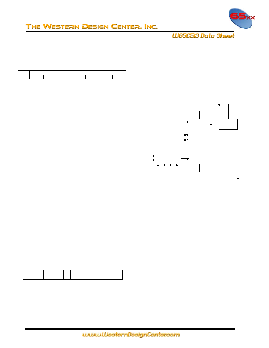
These bits select the Transmitter baud rate, which can be at
1/16 an external clock rate or one of 15 other rates controlled
by the internal baud rate generator.
If the Receiver clock uses the same baud rate at the
transmitter, then RxC becomes an output and can be used to
slave other circuits to the ACIA. Figure 3 shows the
Transmitter and Receiver layout.
RECEIVER
SHIFT REGISTER
CLOCK
DIVIDER
(16)
CONTROL
REGISTER
BIT 4
BAUD RATE
GENERATOR
CLOCK
DIVIDER
(16)
BITS 0-3 IN
CONTROL
REGISTER
TRANSMITTER
SHIFT REGISTER
SYNC
LOGIC
XTLI
XTLO
TxD
RxC
RxD
Figure 4 Transmitter/Receiver Clock Circuits
Receiver Clock Source (Bit 4)
This bit controls the clock source to the Receiver. A 0 causes
the Receiver to operate at a baud rate of 1/16 an external
clock. A 1 causes the Receiver to operate at the same baud
rate as is selected for the transmitter.
Word Length (Bits 5, 6)
These bits determine the word length to be used (5, 6, 7 or 8
bits).
Stop Bit Number (Bit 7)
This bit determines the number of stop bits used. A 0 always
indicates one stop bit. A 1 indicates 1� stop bits if the word
length is 5 with no parity selected, 1 stop bit if the word
length is 8 with parity selected and 2 stop bits in all other
configurations.

7
COMMAND REGISTER
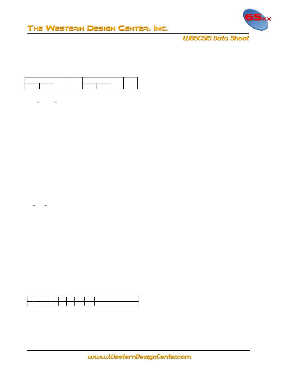
The Command Register controls specific modes and
functions
7
6 5 4
3 2 1 0
PMC TIC
PMC1 PMC0
PME REM
TIC1 TIC0
IRD DTR
Bits 7-6
Parity Mode Control (PMC)
7
6
0 0
Odd
parity
transmitted/received
0
1
Even parity transmitted/received
1
0
Mark parity bit transmitted
Parity check disabled
1
1
Space parity bit transmitted
Parity check disabled
Bit 5
Parity Mode Enabled (PME)
0
Parity mode disabled
No parity bit generated
Parity check disabled
1
Parity mode enabled
Bit 4
Receiver Echo Mode (REM)
0 Receiver
normal
mode
1
Receiver echo mode bits 2 and 3
Must be zero for receiver echo
mode, RTS will be low
Bit 1
Receiver Interrupt Request Disabled (IRD)
0 IRQB
enabled
1 IRQB
disabled
Bit 0
Data Terminal Ready (DTR)
0
Data terminal not ready (DTRB high)
1
Data terminal ready (DTRB low)
Reset Initialization
7 6 5 4 3 2 1 0
0 0 0 0 0 0 0 0 Hardware reset (RESB)
- - - 0 0 0 0 0 Program reset
Data Terminal Ready (Bit 0)
This bit enables all selected interrupts and controls the state
of the Data Terminal Ready (DTRB) line. A 0 indicates the
microcomputer system is not ready by setting the DTRB line
high. A 1 indicates the microcomputer system is ready by
setting the DTRB line low.
Receiver Interrupt Control (Bit 1)
This bit disables the Receiver from generating an interrupt
when set to a 1. The Receiver interrupt is enabled when this
bit is set to a 0 and Bit 0 is set to a 1.
Transmitter Interrupt Control (Bits 2, 3)
These bits control the state of the Ready to Send (RTSB) line
and the Transmitter interrupt.
Receiver Echo Mode (Bit 4)
A 1 enables the Receiver Echo Mode and a 0 enables the
Receiver Echo Mode. When bit 4 is a 1 bits 2 and 3 must be
0. In the Receiver Echo Mode, the Transmitter returns each
transmission received by the Receiver delayed by one-half bit
time.
Parity Mode Enable (Bit 5)
This bit enables parity bit generation and checking. A 0
disables parity bit generation by the Transmitter and parity
bit checking by the Receiver. A 1 bit enables generation and
checking of parity bits.
Parity Mode Control (Bits 6, 7)
These bits determine the type of parity generated by the
Transmitter (even, odd, mark or space) and the type of parity
check done by the Receiver (even, odd or no check).
Bits 3-2
Transmitter Interrupt Control (TIC)
3
2
0
0
RTSB = High, transmit interrupt disabled
0
1
RTSB = Low, transmit interrupt enabled
1
0
RTSB = Low, transmit interrupt disabled
1 1 RTSB = Low, transmit interrupt disabled
Transmit break on TxD

8
INTERFACE SIGNALS
Figure 4 shows the ACIA interface signals associated with
the microprocessor and the modem.
Figure 5 ACIA Interface Diagram
MICROPROCESSOR INTERFACE
Reset (RESB)
During System initialization a low on the RESB input causes
a hardware reset to occur. Upon reset, the Command
Register and the Control Register are cleared (all bits set to
0). The Status Register is cleared with the exception of the
indications of Data Set Ready and Data Carrier Detect, which
are externally controlled by the DSRB and DCDB lines, and
the transmitter Empty bit, which is set. RESB must be held
low for one PHI2 clock cycle for a reset to occur.
Input Clock (PHI2)
The input clock is the system PHI2 clock and clocks all data
transfers between the system microprocessor and the ACIA.
Read/Write (RWB)
The RWB input, generated by the microprocessor controls
the direction of data transfers. A high on the RWB pin
allows the processor to read the data supplied by the ACIA, a
low allows a write to the ACIA.
Interrupt Request (IRQB)
The IRQB pin is an interrupt output from the interrupt
control logic. It is an open drain output, permitting several
devices to be connected to the common IRQB
microprocessor input. Normally a high level, IRQB goes low
when an interrupt occurs.
Data Bus (D0-D7)
The eight data line (D0-D7) pins transfer data between the
processor and the ACIA. These lines are bi-directional and
are normally high-impedance except during Read cycles
when the ACIA is selected.
Chip Selects (CS0, CS1B)
The two chip select inputs are normally connected to the
processor address lines either directly or through decoders.
The ACIA is selected when CS0 is high and CS1B is low.
When the ACIA is selected, the internal registers are
addressed in accordance with the register select lines (RS0,
RS1).
Register Selects (RS0, RS1)
The two register select lines are normally connected to the
processor address lines to allow the processor to select the
various ACIA internal registers. Table 1 shows the internal
register select coding.
Table 1 ACIA Register Selection
Register Operation
RS1 RS0
RWB = Low
RWB = High
L
L
Write Transmit Data
Register
Read Receiver
Data Register
L H
Programmed
Reset
(Data is "Don't
Care")
Read Status
Register
H L
Write
Command
Register
Read Command
Register
H H
Write
Control
Register
Read Control
Register
Only the Command and Control registers can both be read
and written. The programmed Reset operation does not
cause any data transfer, but is used to clear bits 4 through 0 in
the Command Register and bit 2 in the Status Register. The
Control Register is unchanged by a programmed Reset. It
should be noted that the programmed Reset is slightly
different from the hardware Reset (RESB); refer to the
register description.

9
ACIA/MODEM INTERFACE
Crystal Pins (XTLI, XTLO)
These pins are normally directly connected to the external
crystal (1.8432 MHz) to derive the various baud rates.
Alternatively, an externally generated clock can drive the
XTLI pin, in which case the XTLO pin must float. XTLI is
the input pin for the transmit clock.
Transmit Data (TxD)
The TxD output line transfers serial non-return-to-zero
(NRZ) data to the modem. The least significant bit (LSB) of
the Transmit Data Register is the first data bit transmitted and
the rate of data transmission is determined by the baud rate
selected or under control of an external clock. This selection
is made by programming the Control Register.
Receive Data (RxD)
The RxD input line transfers serial NRZ data into the ACIA
from the modem, LSB first. The receiver data rate is either
the programmed baud rate or under the control of an
externally generated receiver clock. The selection is made by
programming the Control Register.
Receive Clock (RxC)
The RxC is a bi-directional pin which is either the receiver
16x clock input or the receiver 16x clock output. The latter
mode results if the internal baud rate generator is selected for
receiver data clocking.
Request to Send (RTSB)
The RTSB output pin controls the modem from the
processor. The state of the RTSB pin is determined by the
contents of the Command Register.
Clear to Send (CTSB)
The CTSB input pin controls the transmitter operation. The
enable state is with CTSB low. The transmitter is
automatically disabled if CTSB is high.
Data Terminal Ready (DTRB)
This output pin indicates the status of the ACIA to the
modem. A low on DTRB indicates the ACIA is enabled, a
high indicates it is disabled. The processor controls this pin
via bit 0 of the Command Register.
Data Set Ready (DSRB)
The DSRB input pin indicates to the ACIA the status of the
modem. A low indicates the "ready" state and a high, "not-
ready"
Data Carrier Detect (DCDB)
The DCDB input pin indicates to the ACIA the status of the
carrier-detect output of the modem. A low indicates that the
modem carrier signal is present and a high, that it is not.
TRANSMITTER AND RECEIVER OPERATION
Continuous Data Transmit
In the normal operating mode, the interrupt request output
(IRQB) signals when the ACIA is ready to accept the next
data word to be transmitted. This interrupt occurs at the
beginning of the Start Bit. When the processor reads the
Status Register of the ACIA, the interrupt is cleared.
The processor must then identify that the Transmit Data
Register is ready to be loaded and must then load it with the
next data word. This must occur before the end of the Stop
Bit, otherwise a continuous "MARK" will be transmitted.
Figure 5 shows the continuous Data Transmit timing
relationship.
CHAR # n
CHAR # n+1
CHAR # n+2
CHAR # n+3
Start
Start
Start
Start
Stop
Stop
Stop
Stop
P
B
N
B
1
B
0
P
B
N
B
1
B
0
P
B
N
B
1
B
0
P
B
N
B
1
B
0
PROCESSOR INTERRUPT
(TRANSMIT DATA
REGISTER EMPTY)
PROCESSOR READS
STATUS REGISTER,
CAUSES IRQB TO CLEAR.
PROCESSOR MUST
LOAD NEW DATA IN THIS
TIME INTERVAL;
OTHERWISE,
CONTINUOUS "MARK" IS
TRANSMITTED
TxD
IRQB
Figure 6 Continuous Data Transmit

10
Continuous Data Receive
Similar to the Continuous Data Transmit case, the normal
operation of this mode is to assert IRQB when the ACIA has
received a full data word. This occurs at about the 9/16
point through the Stop Bit. The processor must read the
Status Register and read the data word before the next
interrupt, otherwise the Overrun condition occurs. Figure 6
shows the continuous Data Receive Timing Relationship.
CHAR # n
CHAR # n+1
CHAR # n+2
CHAR # n+3
Start
Start
Start
Start
Stop
Stop
Stop
Stop
P
B
N
B
1
B
0
P
B
N
B
1
B
0
P
B
N
B
1
B
0
P
B
N
B
1
B
0
PROCESSOR INTERRUPT
OCCURS ABOUT 9/16
INTO LAST STOP BIT.
PARITY, OVERRUN AND
FRAMING ERROR ALSO
UPDATED
PROCESSOR READS
STATUS REGISTER,
CAUSES IRQB TO CLEAR.
PROCESSOR MUST
READ RECEIVER DATA IN
THIS TIME INTERVAL;
OTHERWISE, OVERRUN
OCCURS
RxD
IRQB
Figure 7 Continuous Data Receive
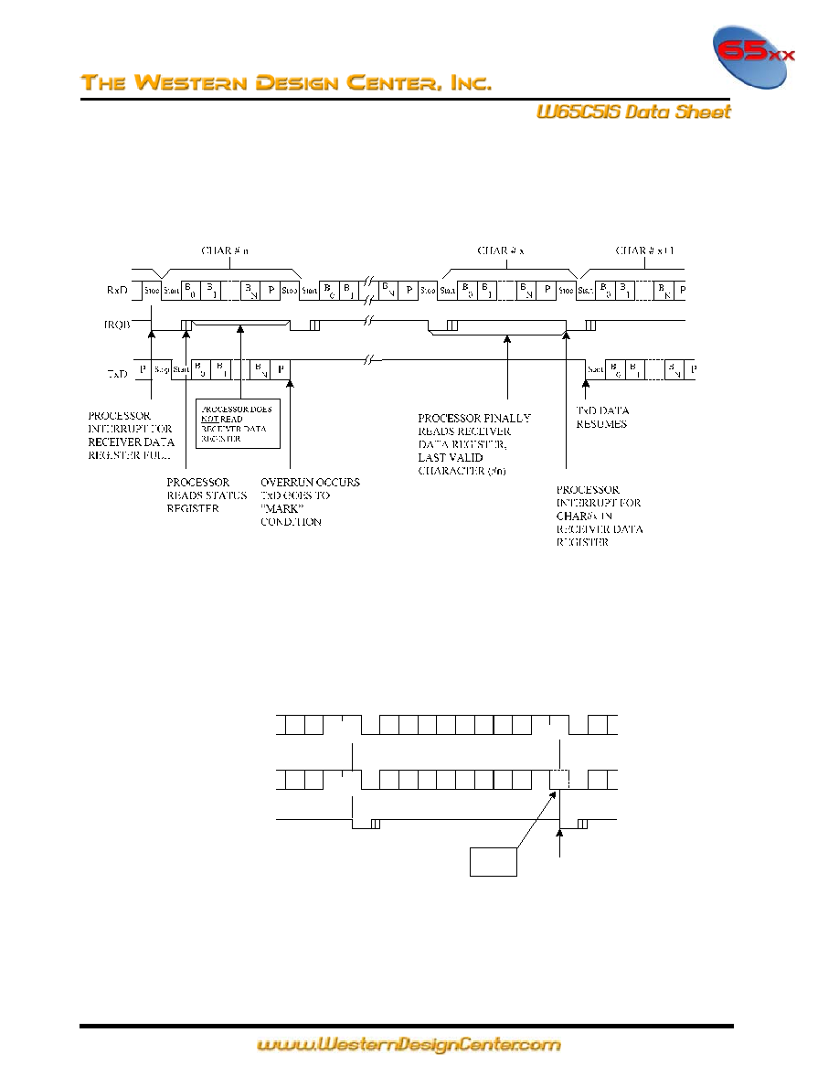
Transmit Data Register Not Loaded by Processor
If the processor is unable to load the Transmit Data Register
in the allocated time, then the TxD line goes to the "MARK"
condition until the data is loaded. IRQB interrupts continue
to occur at the same rate as previously,
except no data is transmitted. When the processor finally
loads new data, a Start Bit immediately occurs, the data word
transmission is started and another interrupt is initiated,
signaling for the next data word. Figure 7 shows the timing
relationship forthis mode of operation.
Figure 8 Transmit Data Register Not Loaded by Processor

11
Effect of CTSB on Transmitter
CTSB is the Clear-to-Send signal generated by the modem.
It is normally low (true state) but may go high in the event of
some modem problems. When this occurs, the TxD line goes
to the "MARK" condition after the entire last character
(including parity and stop bit) have been transmitted. Bit 4
in the Status Register indicates that the Transmitter Data
Register is not empty and IRQB is not asserted. CTSB is
transmit control line only, and has not effect on the ACIA
Receiver Operation. Figure 8 shows the timing relationship
for this mode of operation.
Figure 9 Effect of CTS on Transmitter
Effect of Overrun on Receiver
If the processor does not read the Receiver Data Register in
the allocated time, then, when the following interrupt occurs,
the new data word is not transferred to the Receiver Data
Register, but the Overrun status bit is set. Thus, the
Data Register will contain the last valid data word received
and all following data is lost. Figure 9 shows the timing
relationship for this mode.
Figure 10 Effect of Overrun on Receiver

12
Echo Mode Timing
In Echo Mode, the TxD line re-transmits the data on the RxD
line, delayed by � of the bit time, as shown in Figure 10.
Start
Start
Start
Stop
Stop
Stop
B
0
P
B
N
B
1
B
0
P
B
N
B
1
B
0
RxD
B
0
P
B
N
B
1
B
0
P
B
N
B
1
B
0
Stop Start
Stop Start
Stop Start
TxD
P
� DATA BIT DELAY
Figure 11 Echo Mode Timing
Effect of CTSB on Echo Mode Operation
In Echo Mode, the Receiver operation is unaffected by
CTSB, however, the Transmitter is affected when CTSB goes
high, ie., the TxD line immediately goes to a continuous
"Mark" condition. In this case, however, the
Status Register indicates that the Receiver Data Register is
full in response to an IRQB, so the processor has no way of
knowing that the Transmitter has ceased to echo. See Figure
11 for the timing relationship of this mode.
Figure 12 Effect of CTSB on Echo Mode

13
Overrun in Echo Mode
If Overrun occurs in Echo Mode, the Receiver is affected the
same way as a normal overrun in Receive Mode. For
the retransmitted data, when overrun occurs, the TxD line
goes to the "MARK" condition until the first Start Bit after
the Receiver Data Register is read by the processor. Figure
12 shows the timing relationship for this mode.
Figure 13 Overrun in Echo Mode
Framing Error
Framing Error is caused by the absence of Stop Bit(s) on
received data. A Framing Error is indicated by the setting of
bit 1 in the Status Register at the same time the Receiver
Data Register Full bit is set, also in the Status Register. In
response to IRQB, generated by RDRF, the Status Register
can also be checked for the Framing Error. Subsequent data
words are tested for Framing Error separately, so the status
bit will always reflect the last data word received. See Figure
13 for Framing Error timing relationship.
Start
Start
Stop
Stop
B
0
P
B
3
B
1
B
0
RxD
(EXPECTED)
B
2
B
4
B
5
B
6
Stop
B
6
P
Stop
Start
Start
Stop
Stop
B
0
P
B
3
B
1
B
0
RxD
(ACTUAL)
B
2
B
4
B
5
B
6
Stop
B
6
P
Stop
1
1
1
1
2
2
2
2
IRQB
MISSING
STOP BIT
PROCESSOR
INTERRUPT,
FRAMING
ERROR
BIT SET
NOTES: 1. FRAMING ERROR DOES NOT
INHIBIT RECEIVER OPERATION
2. IF NEXT DATA WORD IS OK,
FRAMING ERROR IS CLEARED
Figure 14 Framing Error

14
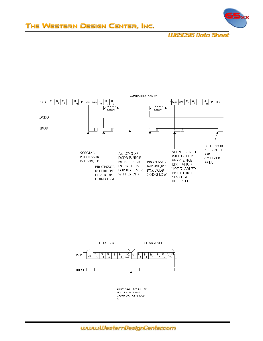
Effect of DCDB on Receiver
DCDB is a modem output indicating the status of the carrier-
frequency-detection circuit of the modem. This line goes
high for a loss of carrier. Normally, when this occurs, the
modem will stop transmitting data some time later. The
ACIA asserts IRQB whenever DCDB changes state and
indicates this condition via bit 5 in the Status Register.
Once such a change of state occurs, subsequent transitions
will not cause interrupts or changes in the Status Register
until the first interrupt is serviced. When the Status Register
is read by the processor, the ACIA automatically checks the
level of the DCDB line, and if it has changed, another IRQB
occurs (see Figure 14).
Figure 15 Effect of DCDB on Receiver
Timing with 1� Stop Bits
It is possible to select 1� Stop Bits, but this occurs only for
5-bit data words with no parity bit. In this case, the IRQB
asserted for Receiver Data Register Full occurs halfway
through the trailing half-Stop Bit. Figure 15 shows the
timing relationship for this mode.
Figure 16 Timing with 1� Stop Bits

15
Transmit Continuous "BREAK"
This mode is selected via the ACIA Command Register and
causes the Transmitter to send continuous "BREAK"
characters, beginning with the next character transmitted. At
least one full "BREAK" character will be transmitted, even if
the processor quickly reprograms the Command Register
transmit mode. Later, when the Command Register is
programmed back to normal transmit mode, an immediate
Stop Bit will be generated and transmission will resume.
Figure 16 shows the timing relationship for this mode.
Note
If, while operating in the Transmit Continuous "BREAK"
mode, the CTSB should go to a high, the TxD will be
overridden by the CTSB and will go to continuous "MARK"
at the beginning of the next character transmitted
after the CTSB goes high.
Figure 17 Transmit Continuous "BREAK"
Receive Continuous "BREAK"
In the event the modem transmits continuous "BREAK"
characters, the ACIA will terminate receiving. Reception
will resume only after a Stop Bit is encountered by the
ACIA. Figure 17 shows the timing relationship for
continuous "BREAK" characters.
Figure 18 Receive Continuous "BREAK"

16
STATUS REGISTER OPERATION
Because of the special functions of the various status bits,
there is a suggested sequence for checking them. When an
interrupt occurs, the ACIA should be interrogated as follows:
1. Read Status Register
This operation automatically clears Bit 7 (IRQB).
Subsequent transitions on DSRB and DCDB will cause
another interrupt.
2. Check IRQB (Bit 7) in the data read from the Status
Register.
If not set, the interrupt source is not the ACIA.
3. Check DCDB and DSRB
These must be compared to their previous levels, which must
have been saved by the processor. If they are both 0 (modem
"on-line") and they are unchanged then the remaining bits
must be checked.
4. Check RDRF (Bit 3)
Check for Receiver Data Register Full.
5. Check Parity, Overrun and Framing Error (Bits 0-2) if the
Receiver Data Register is full.
6. Check TDRE (Bit 4)
Check for Transmitter Data Register Empty.
7. If none of the above conditions exist, then CTSB must
have gone to the false (high) state.
PROGRAM RESET OPERATION
A program reset occurs when the processor performs a write
operation to the ACIA with RS0 low and RS1 high. The
program reset operates somewhat different from the hardware
reset (RESB pin) and is described as follows:
1. Internal registers are not completely cleared. Check
register formats for the effect of a program reset on internal
registers
2. The DTRB line goes high immediately.
3 Receiver and transmitter interrupts are disabled
immediately. If IRQB is low when the reset occurs, it stays
low until serviced, unless interrupt was caused by DCDB or
DSRB transition.
4. DCDB and DSRB interrupts are disabled immediately. If
IRQB is low and was caused by DCDB or DSRB, then it
goes high, also DCDB and DSRB status bits subsequently
will
follow the input lines, although no interrupt will occur.
5. Overrun cleared, if set.
MISCELLANEOUS
1. If Echo Mode is selected, RTSB goes low.
2. If Bit 0 of Command Register is 0 (disabled) then:
a) All interrupts are disabled including those caused by
DCDB and DSRB transitions.
b) Transmitter is disabled immediately.
c) Receiver is disabled, but a character currently being
received will be completed first.
3. Odd parity occurs when the sum of all the 1 bits in the
data word (including the parity bit) is odd.
4. In the receive mode, the received parity bit does not go
into the Receiver Data Register, but generates parity error or
no parity error for the Status Register.
5. Transmitter and Receiver may be in full operation
simultaneously. This is "full-duplex" mode.
6. If the RxD line inadvertently goes low and then high right
after a Stop Bit, the ACIA does not interpret this as a Start
Bit, but samples the line again halfway into the bit to
determine if it is a true Start Bit or a false one. For false Start
Bit detection, the ACIA does not begin to receive data,
instead, only a true Start Bit initiates receiver operation.
7. Precautions to consider with the crystal oscillator circuit:
a) The external crystal should be a "series" mode crystal.
b) The XTLI input may be used as an external clock
input. The unused pin (XTLO) must be floating and may
not be used for any other function.
8. DCDB and DSRB transitions, although causing
immediate processor interrupts, have no affect on transmitter
operation. Data will continue to be sent, unless the processor
forces transmitter to turn off. Since these are high-
impedance inputs, they must not be permitted to float (un-
connected). If unused, they must be terminated either to
GND or Vcc.
GENERATION OF NON-STANDARD BAUD
RATES
Divisors
The internal counter/divider circuit selects the appropriate
divisor for the crystal frequency by means of bits 0-3 of the
ACIA Control Register, as shown in Table 2.
Generating Other Baud Rates
By using a different crystal, other baud rates may be
generated. These can be determined by:
Furthermore, it is possible to drive the ACIA with an off-chip
oscillator to achieve other baud rates. In this case, XTLI (Pin
6) must be the clock input and XTLO (pin 7) must be a no-
connect.

17
Table 2 Divisor Selection
13,704
16,769
24,576
36,864
1,536
3,072
6,144
12,288
256
384
512
1,024
768
96
192
16 x External Clock at Pin RxC
1.8432x 10
6
12,288
1.8432x 10
6
36,864
1.8432x 10
6
768
1.8432x 10
6
1,024
1.8432x 10
6
1,536
1.8432x 10
6
3,072
1.8432x 10
6
6,144
1.8432x 10
6
13,704
1.8432x 10
6
192
1.8432x 10
6
256
1.8432x 10
6
384
1.8432x 10
6
512
1.8432x 10
6
96
16 x External Clock at Pin RxC
F
36,864
Control
Register
Bits
Divisor Selected
for the Internal
Counter
Baud Rate
Generated With
1.8432MHz Crystal
Baud Rate
Generated With a
Crystal of
Frequency (F)
3 2 1 0
0 0 0 0
0 0 0 1
0 0 1 0
0 0 1 1
0 1 0 0
0 1 0 1
0 1 1 1
1 0 0 0
1 0 0 1
1 0 1 0
1 0 1 1
1 1 0 1
1 1 0 0
1 1 1 0
1 1 1 1
0 1 1 0
No Divisor Selected
=50
1.8432x 10
6
24,576
=75
1.8432x 10
6
16,769
F
24,576
F
16,769
F
13,704
F
12,288
F
6,144
F
3,072
F
1,536
F
1,024
F
768
F
512
F
384
F
256
F
192
F
96
=109.92
=134.51
=150
=300
=600
=1,200
=1,800
=2,400
=3,600
=4,800
=7,200
=9,600
=19,200

18
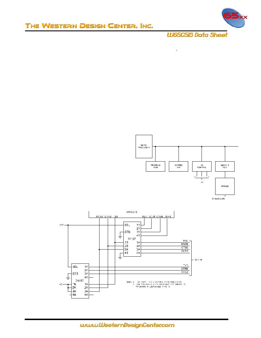
DIAGNOSTIC LOOP-BACK OPERATING MODES
A simplified block diagram for a system incorporating an
ACIA is shown in Figure 18.
It may be desirable to include in the system a facility for
"loop-back" testing, of which there are two kinds.
1.
Local Loop-Back
Loop-back from the point of view of the processor.
In this case, the Modem and Data Link must be
effectively disconnected and the ACIA transmitter
connected back to its own receiver, so that the
processor can perform diagnostic checks on the
system, excluding the actual data channel.
2.
Remote Loop-back
Loop-back from the point of view of the Data Link
and Modem. In this case, the processor, itself, is
disconnected and all received data is immediately
retransmitted, so the system on the other end of the
Data Link may operate independent of the local
system.
The ACIA does not contain automatic loop-back
operating modes, but they may be implemented with the
addition of a small amount of external circuitry. Figure
19 indicates the necessary logic to be used with the
ACIA. The LBB line is the positive-true signal to enable
local loop-back operation. Essentially, LLB = high does
the following:
1. Disables outputs TxD, DTRB and RTSB (to Modem)
2. Disables inputs RxD, DCDB, CTSB, DSRB (from
Modem)
3. Connects transmitter outputs to respective receiver
inputs (i,e., TxD to RxD, DTRB to DCDB, RTSB to
CTSB).
LLB may be tied to a peripheral control pin (from a
W65C21 or W65C22S, for example) to provide processor
control of local loop-back operation. In this way, the
processor can easily perform local loop-back diagnostic
testing.
Remote loop-back does not require this circuitry, so LLB
must be set low. However, the processor must select the
following:
1. Control Register bit 4 must be 1, so that the
transmitter clock equals the receiver clock.
2. Command Register bit 4 must be 1 to select Echo
Mode.
3. Command Register bits 3 and 2 must be 1 and 0,
respectively to disable IRQB interrupt to transmitter.
4. Command Register bit 1 must be 0 to disable IRQB
interrupt for receiver.
In this way, the system re-transmits received data without
any effect on the local system.
Figure 19 Simplified System Diagram
Figure 20 Loop-Back Circuit Schematic

19
READ TIMING DIAGRAM
Timing diagrams for transmit with external
clock, receive with external clock and IRQB
generation are shown in Figures 20, 21 and 22
respectively. The corresponding timing
characteristics are listed in Table 3.
Table 3 Transmit/Receive Characteristics
1 MHz
2 MHz
Characteristic Symbol
Min Max Min Max
Unit
Transmit/Receive
Clock Rate
t
CCY
400* - 400* -
nS
Transmit/Receive
Clock High Time
t
CH
175 - 175 -
nS
Transmit/Receive
Clock Low Time
t
CL
175 - 175 -
nS
XTLI to TxD
Propagation Delay
t
DD
- 500 - 500 nS
RTS Propagation
Delay
t
DLY
- 500 - 500 nS
IRQB Propagation
Delay (Clear)
t
IRQ
- 500 - 500 nS
Notes:
1. (t
R
, t
F
= 10 to 30 nS)
*
The baud rate with external clocking is: Baud Rate = 1
16 x t
CCY
Test and Crystal Specifications
1. Temperature stability � 0.01% (-40� C to +85� C)
2. Characteristics at 25� C � 2� C
a. Frequency (MHz)
1.8432
b. Frequency tolerance (� %)
0.02
c. Resonance mode
Series
d. Equivalent resistance (ohm) 400 max.
e. Drive level (mW)
2
f. Shunt capacitance (pF)
7 max.
g. Oscillation mode
Fundamental
Figure 21 Clock Generation W65C51S
Figure 22 Transmit Timing with External Clock
Figure 23 Receive External Clock Timing
t
DLY
t
IRQ
PHI2
DTRB, RTSB
IRQB
(CLEAR)
Figure 24 Interrupt and Output Timing
30pF
XTLI
XTLO
1MO
6
7
XTLI
XTLO
7
6
INTERNAL CLOCK
EXTERNAL CLOCK
OPEN
CIRCUIT
EXTERNAL
CLOCK

20
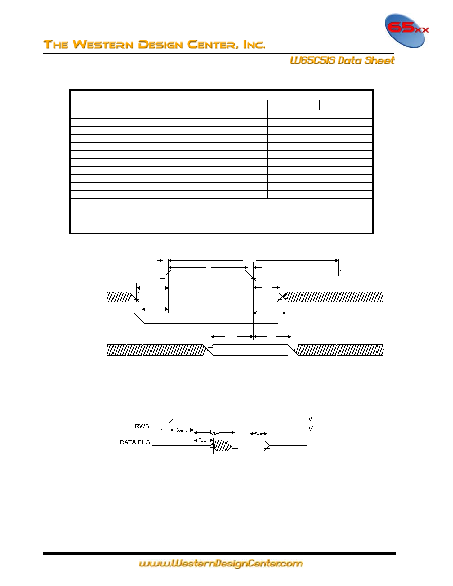
Table 4 AC Characteristics
2 MHz
4 MHz
Parameter Symbol
Min Max Min Max
Units
PHI2 Cycle Time
t
CYC
500 - 250 -
nS
PHI2 Pulse Width
t
C
200 - 100 -
nS
Address Set-Up Time
t
AC
60 - 30 -
nS
Address Hold Time
t
CAH
0 - 0 -
nS
RWB Set-Up Time
t
WC
60 - 30 -
nS
RWB Hold Time
t
CWH
0 - 0 -
nS
Data Bus Set-Up time
t
DCW
60 - 35 -
nS
Data Bus Hold Time
t
HW
10 - 5 -
nS
Read Access Time (Valid Data)
t
CDR
- 150 - 50
nS
Read Hold Time
t
HR
10 - 10 -
nS
Bus Active Time (Invalid Data)
t
CDA
20 - 10 -
nS
Notes:
1. V
CC
= 5.0V � 5%
2. T
A
= T
L
to T
H
3. t
R
and t
F
= 10 to 30 nSs.
t
R
t
C
t
CYC
t
F
t
ACW
t
CAH
t
CWH
t
WCW
t
DCW
t
HW
V
IH
V
IL
V
IH
V
IL
PHI2
CS0, CS1B, RS0
RS1
RWB
DATA BUS
V
IH
V
IL
V
IL
V
IH
Figure 25 Write Timing Diagram
Figure 26 Read Timing Characteristics

21
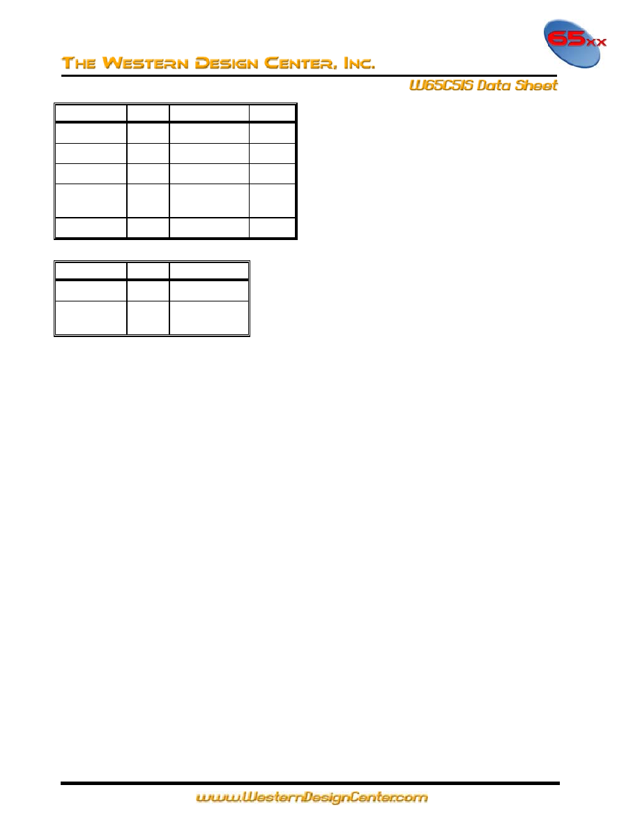
ABSOLUTE MAXIMUM RATINGS*
Parameter Symbol
Value
Unit
Supply Voltage
V
CC
-0.3 to +7.0V
Vdc
Input Voltage
V
IN
-0.3 to V
CC
+0.3
Vdc
Output Voltage
V
OUT
-0.3 to V
CC
+0.3V
Vdc
Operating Temp.
Commercial
Industrial
T
A
0 to +70
-40 to +85
�C
Storage Temp.
T
STG
-55 to +150
�C
OPERATING CONDITIONS
Parameter Symbol
Value
Supply Voltage
V
CC
5V � 5%
Operating Temp.
Commercial
Industrial
T
A
0 to +70�C
-40�C to +85�C
*
NOTE: Stresses above those listed may cause permanent
damage to the device. This is a stress rating only and
functional operation of the device at these or any other
conditions above those indicated in other sections of this
document is not implied. Exposure to absolute maximum
rating conditions for extended periods may affect device
reliability.

3/7/2006
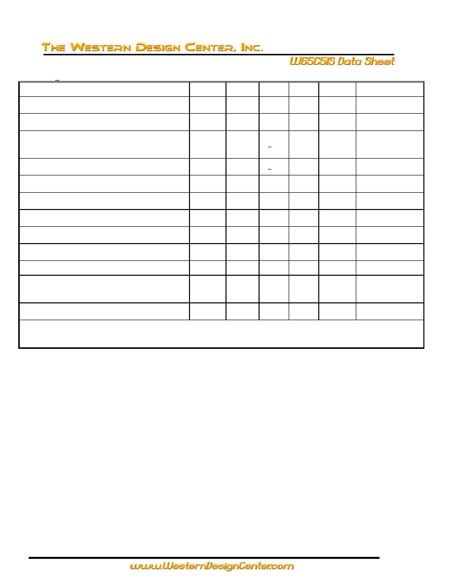
DC CHARACTERISTICS
(V
CC
= 5.0V + 5%, V
SS
= 0, T
A
= T
L
to T
H
, unless otherwise noted)
Parameter Symbol
Min
Typ
Max
Unit
Test
Conditions
Input High Voltage
V
IH
2.0 -- V
CC
V
Input Low Voltage
V
IL
-0.3
-- +0.8
V
Input Leakage Current
CS0, CS1B, CTSB, DCDB, DSRB, PHI2, RESB,
RS0, RS1, RWB, RxD
I
IN
-- +1 �2.5
�A
V
IN
= 0V to V
CC
V
CC
= 5.25V
Leakage Current (Three State Off)
D0-D7
I
TSI
-- +2 �10 �A
V
IN
= 0.4V to 2.4V
V
CC
= 5.25V
Output High Voltage
D0-D7, DTRB, RTSB, RxC, TxD
V
OH
2.4 -- -- V
V
CC
= 4.75V
I
LOAD
= -100 �A
Output Low Voltage
D0-D7, DTRB , IRQB, RTSB, RxC, TxD,
V
OL
-- -- 0.4
V
V
CC
= 4.75V
I
LOAD
= 1.6 mA
Output High Current (Sourcing)
D0-D7, DTRB, RTSB, RxC, TxD
I
OH
-200
-400
--
�A V
OH
= 2.4V
Output Low Current (Sinking)
D0-D7, DTRB , IRQB, RTSB, RxC, TxD,
I
OL
1.6 -- -- mA V
OL
= 0.4V
Output Leakage Current (off state): IRQB
I
OFF
-- 10
�A V
OUT
= 5.0V
Power Dissipation
P
D
-- 7
10
mW/MHz
Input Capacitance
All except PHI2
PHI2
C
CLK
C
IN
--
--
20
10
pF
pF
V
CC
= 5.0V
V
IN
= 0V
f = 2 MHz
T
A
= 25
C
Output Capacitance
C
OUT
-- 10 pF
Notes:
1. All units are direct current (dc) except for capacitance.
2. Negative sign indicates outward current flow, positive indicates inward flow.
3. Typical values are shown for V
CC
= 5.0V and TA = 25
C

23
Figure 27 28 Pin Plastic Dip Package Dimensions

24
ORDERING INFORMATION
W65C51S6TPG-14
Description
W65C
W65C = standard product
Product Identification Number
51S
Foundry Process
6T = 0.6u TSMC Process
6T
Package
P = Plastic Dual-In-Line, 28 pins
P
RoHS/Green Compliance
G = RoHS/Green Compliant (Wafer and Packaging)
G
Speed Designator
-14 = 14MHz
-14
___________________________________________________________________________
To receive general sales or technical support on standard product or information about our module
library licenses, contact us at:
The Western Design Center, Inc.
2166 East Brown Road
Mesa, Arizona 85213 USA
Phone: 480-962-4545 Fax: 480-835-6442
e-mail: information@westerndesigncenter.com
www.westerndesigncenter.com
_____________________________________________________________________________
WARNING: MOS CIRCUITS ARE SUBJECT TO DAMAGE FROM STATIC ELECTRICAL
CHARGE BUILDUPS. Industry established recommendations for handling MOS circuits include:
1.
Ship and store product in conductive shipping tubes or conductive foam plastic. Never ship or
store product in non-conductive plastic containers or non-conductive plastic foam material.
2.
Handle MOS parts only at conductive workstations.
3.
Ground all assembly and repair tools.

25
W65C51S6 Samples Errata Sheet for Lot SA1105A
Note: The internal feedback resistor was removed from the W65C51S6 and therefore an external
feedback resistor is required between XTLI (aka XTAL1) and XTLO (XTAL2).
This document will describe the current known errors with the W65C51 ACIA Engineering
Samples found by WDC. Please contact WDC with any other errors found while evaluating these
samples.
Internal Oscillator Problem.
The internal crystal oscillator does not function properly on these samples; an external oscillator
that drives XTLI (aka XTAL1) is required for full functional operation.
Transmit Data Register Empty Problem.
The following issue was found relating to transmitting on TxD. The transmitter was found to be
working as outlined in the data sheet, however bit 4 of the Status Register (Transmit Data Register
Empty) remains a 0 when it should be a 1 after the first byte of a string is written to the Transmit
Data Register, therefore the first byte is transmitted twice. As long as the transmitter is reloaded
when the transmitter is transmitting bit 4 of the status register seems to work properly.
Software Work Around for Transmit Data Register Empty Problem.
We have found that if after first setting bits 2 and/or 3 of the Command Register to enable
transmitting, immediately begin storing the data to be transmitted in the Transmit Data Register bit
4 of the Status Register works properly if the Transmitter Data Register is written to within 1 bit
time (16 cycles of the baud rate clock). Many designs may have operated this way in order to
reduce power consumption. An example is provided below:
SNDLN:
lda
#%00001000
;Turn
on
transmitter
sta
CommandRegister
lda StatusRegister
;Check to make sure the
and
#%00010000
;Transmit Data Register
beq
SNDLN
;is
empty
lda
signon,x
;send
a
character
sta TxD
inx
cmp #$0D
;Yes - Is this the last char
bne SNDLN
;No - Send the next one
lda
#%00000001
;Turn
off
transmitter
sta CommandRegister
;and turn on reciever
bra MNLOOP
;Yes - Get the next line

26
W65C51S6 Samples Errata Sheet for Lot SA0519A
Note: The internal feedback resistor was removed from the W65C51S6 and therefore an external
feedback resistor is required between XTLI (aka XTAL1) and XTLO (XTAL2).
This document will describe the current known errors with the W65C51 ACIA Engineering
Samples found by WDC. Please contact WDC with any other errors found while evaluating these
samples.
Internal Oscillator Problem.
The internal crystal oscillator does not function properly on these samples; an external oscillator
that drives XTLI (aka XTAL1) is required for full functional operation.
Initial Transmit Shift Register.
After reading the receive register, determining that the transmit data register is empty and sending a
stream of characters to the transmit data register, the initial one or two writes to the transmitter may
intermittently shift incorrectly depending on the circuit design used.


