
Mar. 2002
1
ZC0302
VGA & CIF USB PC Camera Controller
ZC0302
VGA USB PC Camera Processor
Vimicro Corporation
Data Sheet
Vimicro
Corporation reserves the right to make changes without further notice to any product herein to improve
reliability, function or design.
Vimicro
does not assume any liability arising out of the application or use of any
project, circuit described herein; neither does it convey any license under its patent nor the right of others.
This document contains information of a proprietary nature. None of this information shall be divulged to persons
other than
Vimicro
Corporation employee authorized by the nature of their duties to receive such information, or
individuals or organizations authorized by
Vimicro
Corporation.

Mar. 2002
2
ZC0302
VGA & CIF USB PC Camera Controller
Contents
1. Features 4
1.1. General Features
4
2. Architecture
5
2.1. ZC0302 Block Diagram
5
2.2. CMOS Image Sensor Interfaces
5
2.3. USB Features
6
2.4. Image Signal Processing
6
2.5. Raster
6
2.6. Compression Engine
6
2.7. Audio Interface
6
2.8. System Controller
6
3. Pin Definition
8
3.1. Pin Assignment
8
3.2. Pin Description
8
4. Electrical Characteristics
10
4.1. Absolute Maximum Ratings
10
4.2. DC Characteristics
10
4.3. USB Transceiver AC Characteristics
10
4.4. RESET Timing AC Characteristics
11
4.5. Clock AC Characteristics
11
4.6. Input Signal AC Characteristics
12
4.7. Output Signal AC Characteristic
12
5. Mechanical Information 13
6. Appendix 13

Mar. 2002
3
ZC0302
VGA & CIF USB PC Camera Controller
Illustrations
Figure 1 USB PC Camera System Block Diagram
3
Figure 2 Block diagram of ZC0302
5
Figure 3 48-Pin LQFP Package
8
Figure 4 RESET Timing AC Characteristics Diagram
11
Figure 5 Clock Timing AC Characteristics Diagram
11
Figure 6. Input signal AC characteristics
12
Figure 7. VSYNC/HSYNC output AC characteristics
12
Figure 8. 48-Pin LQFP Package Diagram (OMITTED)
13
Figure 9. Serial Bus Timing Diagram
13
Tables
Table 3.1 ZC0302 Pin Descriptions
8
Table 4.1 Absolute Maximum Ratings
10
Table
4.2
DC
Characteristics
10
Table 4.3 Full-Speed Driver Electrical Characteristics
10
Table 4.4 Low-Speed Driver Electrical Characteristics
10
Table 4.5 Reset Signal AC Characteristics
11
Table 4.6 Clock Signal AC Characteristics
11
Table 4.7 CS_D input signal AC Characteristics
12
Table 4.8 Vsync / Hsync input AC Characteristics
12
Table 4.9 Vsync / Hsync output AC characteristics
13
Table 5.1 ZC0302 Package Dimension
13
Table 7. Serial Bus Timing Table
14
Mar. 2002
4
ZC0302
VGA & CIF USB PC Camera Controller
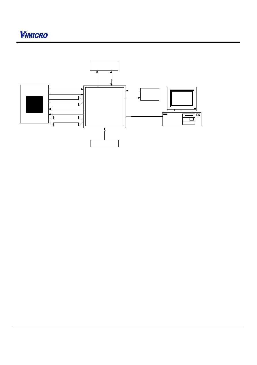
1. Features
PC
ZC0302
DATA[8:0]
Serial Interface
VSYNC
HSYNC
PCLK
ENB
CRYSTAL
48M Hz
CMOS IMAGE SENSORS
USB CABLE
EEPROM
ES
CK
ES
DA
MIC
OSCIN
OSCOUT
F
IGURE
1 USB PC C
AMERA
S
YSTEM
B
LOCK
D
IAGRAM
The ZC0302 chip provides a cost effective single chip solution for the PC camera application. It communicates with
PC host via Universal Serial Bus (USB) port. All major image processing functions, such as image signal
processing (ISP), image data compression and data transfer units are built in the chip. Meanwhile ZC0302 also
provides high quality audio sampling function for sound recording. The audio function complies with USB audio class
1.0.
ZC0302 is designed as a cost-effective single-chip device replacing the complex and costly chip sets used in current
PC camera designs with embedded USB device controller and transceiver, 48-QFP package, and no external
DRAM requirement. Advanced on-chip image signal processor and JPEG encoder produce images with superior
quality.
1.1. General Features
Low cost, single chip solution for high resolution USB PC camera applications
Audio function complying to USB audio device class 1.0
Support up to 15 fps VGA video display without DRAM
USB Device Controller compliant with USB protocol 1.1
USB parameter configurable through EEPROM
Support 9/8-bit RGB Bayer pattern raw data input from CMOS image sensors
Support programmable color correction and gamma correction
Support programmable Auto Exposure/Auto White Balance
Support Auto Gain Control
Support ISO/IEC 10918-1 (JPEG) standard image compression
Support 4 quantization tables for programmable image quality
Support raw data output for high quality still image
3.3V I/O, 2.5V core
No external DRAM required
Flexible system level solution support
Mar. 2002
5
ZC0302
VGA & CIF USB PC Camera Controller
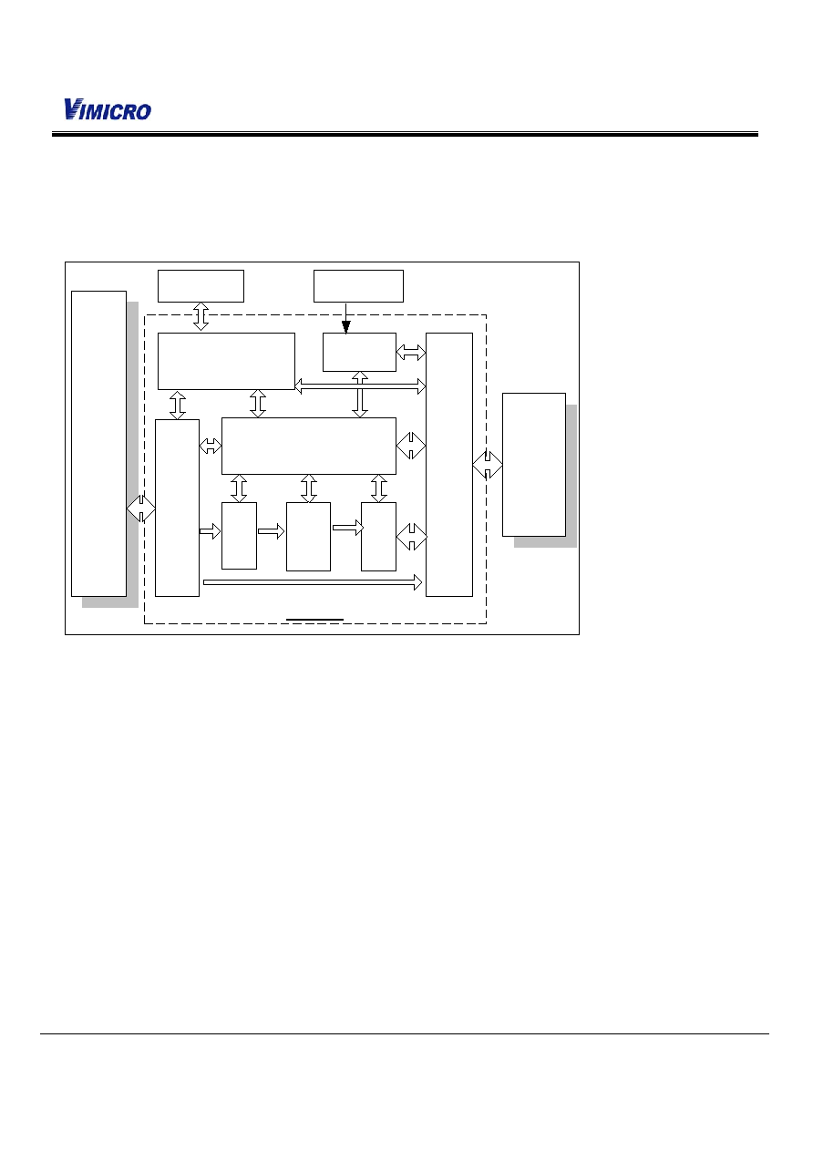
2. Architecture
2.1. ZC0302 Block Diagram
CIS
(
C
M
O
S Im
ag
e Sens
o
r
)
PC
HOST
ZC0302
UD
C
(USB Device
Co
nt
roller)
System Controller
CIS
Interface
Audio
Interface
Subs
ample
&
Ras
t
er
JP
EG
Enc
ode
r
ISP
EEPROM
Interface
EEPROM
MIC
F
IGURE
2 B
LOCK DIAGRAM OF
ZC0302
Figure 2 shows the block diagram of ZC0302. The ISP block receives RGB raw data from CMOS image sensor
interface and performs various image processing tasks such as white balance, color correction, gamma correction,
histogram equalization and so on. The Sub-sample & Raster block handles the input image data scaling and
converts input image data to 8x8 block data format required by DCT module. The JPEG Encoder block compresses
the image data from ISP block into JPEG format data. The compressed image data is then transferred to PC host
via USB Device Controller (UDC) block for display.
The Audio Interface takes the audio input in mono 16-bit PCM format, and then transfers it to PC Host through the
audio streaming pipe in UDC.
2.2. CMOS Image Sensor Interfaces
Support sensors from most CMOS image sensor vendors including Agilent, Hynix, IC Media, TASC, PixArt,
Photobit, OmniVision, and Century
9bit/8bit camera input interface

Mar. 2002
6
ZC0302
VGA & CIF USB PC Camera Controller
2.3. USB Features
Built-in USB transceiver
Suspend and Remote wakeup
3 interface for video, audio and control
Programmable OEM USB parameters by EEPROM including: vendor ID, product ID, MaxPower, serial Number,
manufacture descriptor, product descriptor and chip revision.
2.4. Image Signal Processing
Hardware Dead Pixel Detection/Concealment
8/9-bit RGB raw data input from CMOS image sensor
2-wire/3-wire serial bus interface to CMOS image sensor
Programmable white balance, color correction and gamma correction
Support automatic Exposure Control, automatic White Balance, automatic CMOS Reset Level Control,
automatic Gain Control and auto/manual Histogram Equalization
Support programmable AE/AWB windows
Support edge enhancement and noise removal
Support 2x2 Sub-Sampling
2.5. Raster
The output data format is 4:2:2 YCbCr
Change the input image data to 8x8 block data format required by the DCT
2.6. Compression Engine
Standard JPEG compression engine comply to ISO/IEC 10918-1 (JPEG)
2 AC and 2 DC Huffman code table
4 quantization tables for different image quality
Adjustable compression rate by Bit Rate Control (BRC) engine
Simplified JPEG header for better performance are programmable
VGA @ 15fps, CIF/SIF up to 30 fps
Adjustable frame rate for efficient bandwidth usage
2.7. Audio Interface
Built-in 16-bit mono audio ADC for audio recording through microphone
Sampling rate @ 8K/16K Hz
USB audio device class 1.0 compliance
2.8. System Controller
Providing the control to ISP, JPEG, and USB blocks
Configuring the control registers
Chip clock generation

Mar. 2002
7
ZC0302
VGA & CIF USB PC Camera Controller
Error detection and handling through USB interface
Mar. 2002
8
ZC0302
VGA & CIF USB PC Camera Controller
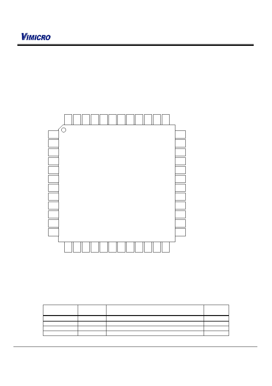
3. Pin Definition
3.1. Pin Assignment
ZSMC
ZC0302 � 48 LQFP
3
CS_D[6]
4
CS_D[5]
1
CS_D[8]
2
CS_D[7]
8
CS_D[3]
9
CS_D[2]
5
NC
7
CS_D[4]
11
CS_D[0]
12
PWUP_RST
10
CS_D[1]
6
NC
C
L
KXIN
13
C
L
KXO
UT
14
DV
SS
15
VS
S_USB
16
DP
17
DM
18
VD
D_
U
S
B
19
SUSP
E
N
DB
21
DV
DD
22
SNAPB
23
GN
D_
A
24
NC
20
32 PIO[0]
31 TEST
30 NC
29 VCM
28 VREFOUT
27 GND_REF
26 MIC
25 VDD_A
35 ESCK
34 PIO[2]
33 PIO[1]
36 PIO[3]
40
HS
YNC
41
OVSS
42
CS_
C
L
K
43
OV
DD
45
SC
K
46
SDA
47
CS_
E
N
48
CS_
R
ST
B
37
ES
DA
38
CS_
P
WD
B
39
VS
YNC
44
NC
F
IGURE
3 48-P
IN
LQFP P
ACKAGE
3.2. Pin Description
Pin
Type
Function
48 Pin
LQFP
CS_D[8]
I, PD
Sensor data
1
CS_D[7]
I, PD
Sensor data
2
CS_D[6]
I, PD
Sensor data
3
CS_D[5]
I, PD
Sensor data
4
Mar. 2002
9
ZC0302
VGA & CIF USB PC Camera Controller
Pin
Type
Function
48 Pin
LQFP
CS_D[4]
I, PD
Sensor data
7
CS_D[3]
I, PD
Sensor data
8
CS_D[2]
I, PD
Sensor data
9
CS_D[1]
I, PD
Sensor data
10
CS_D[0]
I, PD
Sensor data
11
PWUP_RST
I, Schmitt
Power on reset, active low
12
CLKXIN I
Crystal
input
13
CLKXOUT O
Crystal
output
14
DVSS P Core
ground
15
VSS_USB P
USB
transceiver
ground
16
DP I/O
USB
data
17
DM I/O
USB
data
18
VDD_USB P
USB
transceiver
power
19
SUSPENDB O
Active-low
suspend
21
DVDD P Core
power
22
SNAPB
I, PU
Snapshot and remote wake up, active low
23
GND_A
P
IADC analog ground
24
VDD_A
P
IADC analog power
25
MIC A IADC
microphone
input
26
GND_REF
A
IADC input ground reference
27
VREFOUT A
IADC
reference
voltage
28
VCM
A
IADC common-mode voltage
29
TEST
I, PD
Manufacturing test mode
31
PIO[0]
I/O, PD
General purpose I/O
32
PIO[1]
I/O, PD
General purpose I/O
33
PIO[2]
I/O, PD
General purpose I/O
34
ESCK
O
SEEPROM clock
35
PIO[3]
I/O, PD
General purpose I/O
36
ESDA
I/O, Schmitt
EEPRPOM data
37
CS_PWDB
O
Power-down pin controlling DC/DC regulator
38
VSYNC
I/O, PD
Vertical synchronous signal
39
HSYNC
I/O, PD
Horizontal synchronous signal
40
OVSS P I/O
ground
41
OVSS P I/O
ground
41
CS_CLK
O
Sensor clock
42
OVDD P I/O
power
43
SCK / SICLK
O, PD
Serial interface clock
45
SDA / SIVAL
I/O, Schmitt
Serial interface data
46
CS_ENB / SI_EN O, PD
Sensor power enable / Serial interface enable
47
CS_RSTB /
AECNT
O, PD
Sensor reset / auto exposure for TASC VGA sensor
48
T
ABLE
3.1 ZC0302 P
IN
DESCRIPTIONS
Mar. 2002
10
ZC0302
VGA & CIF USB PC Camera Controller
4. Electrical Characteristics
4.1. Absolute Maximum Ratings
Ambient temperature
0oC to 70oC
Storage temperature
-40oC to 125oC
DC supply voltage
3.0V to 3.6V
I/O pin voltage with respect to VSS
-0.3V to VDD + 0.3V
T
ABLE
4.1
A
BSOLUTE
M
AXIMUM
R
ATINGS
4.2. DC Characteristics
Symbol
Parameter
Conditions
Min
Max
Unit
VDD3V
3.3V Power Supply
3.0
3.6
V
VDD2V
2.5V Power Supply
2.25
2.75
V
V
il
Input Low voltage
-0.5
1.0
V
V
ih
Input High voltage
2.3
5.5
V
V
ol
Output Low Voltage
-
0.4
V
V
oh
Output High Voltage
2.4
-
V
I
pd
Suspend current
-
500
uA
I
do
Active current
-
80
mA
T
ABLE
4.2
DC C
HARACTERISTICS
4.3. USB Transceiver AC Characteristics
Symbol
Parameter
Conditions
Min Typ
Max
Unit
T
FR
Rise time
CL=50p
4
20
ns
T
FF
Fall
time
CL=50p
4
20
ns
T
FRFF
Rise and fall
time matching
T
LRLF
=T
LR
/T
LF
90
111.11
%
T
ABLE
4.3
F
ULL
-S
PEED
D
RIVER
E
LECTRICAL
C
HARACTERISTICS
Symbol
Parameter
Conditions
Min Typ Max
Unit
T
LR
Rise time
CL=50p
CL=600p
75
300
ns
T
LF
Fall time
CL=50p
CL=600p
75
300
ns
Mar. 2002
11
ZC0302
VGA & CIF USB PC Camera Controller
T
LRLF
Rise and fall time
matching
T
LRLF
=T
LR
/T
LF
80 125
%
T
ABLE
4.4
L
OW
-S
PEED
D
RIVER
E
LECTRICAL
C
HARACTERISTICS
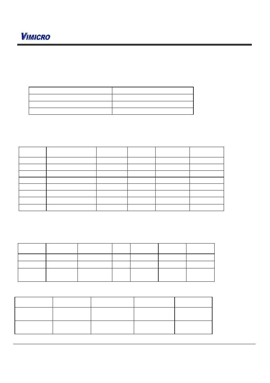
4.4. RESET Timing AC Characteristics
F
IGURE
4 RESET T
IMING
AC C
HARACTERISTICS
D
IAGRAM
Symbol
Parameter
Conditions Min
Max
Unit
T
rst
Reset Pulse Width
--
20
ms
T
ABLE
4.5
R
ESET
S
IGNAL
AC C
HARACTERISTICS
4.5. Clock AC Characteristics
F
IGURE
5 C
LOCK
T
IMING
AC C
HARACTERISTICS
D
IAGRAM
Symbol
Parameter
Conditions Min
Max
Unit
1/Tcyc
Oscillator
Frequency
48@10PPM
-
-
Mhz
T
high
Oscillator Clock
High Time
8.3
-
Ns
Mar. 2002
12
ZC0302
VGA & CIF USB PC Camera Controller
T
low
Oscillator Clock
Low Time
8.3
-
Ns
T
ABLE
4.6
C
LOCK
S
IGNAL
AC C
HARACTERISTICS
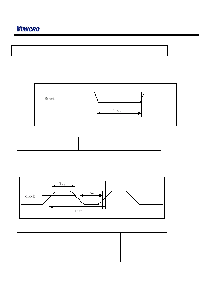
4.6. Input Signal AC Characteristics
CS_CLK
CS_D
Valid data
Tsu
T
h
CS_CLK
Tsu
T
h
V
SYNC
/H
SYNC
F
IGURE
6. I
NPUT SIGNAL
AC
CHARACTERISTICS
Symbol
Parameter Conditions
Min Max
Unit
T
su
Input
setup
time
45
ns
T
h
Input hold time
0
-
ns
TABLE 4.7 CS_D
INPUT SIGNAL
AC
C
HARACTERISTICS
Symbol
parameter conditions
Min Max
Unit
T
su
Input
setup
time
20
ns
T
h
Input hold time
0
-
ns
TABLE 4.8 V
SYNC
/ H
SYNC INPUT
AC C
HARACTERISTICS
4.7. Output Signal AC Characteristic
CS_CLK
T
d
V
SYNC
/H
SYNC
FIGURE 7. VSYNC/HSYNC
OUTPUT
AC
CHARACTERISTICS
Symbol
Parameter Conditions
Min Max
Unit
T
d
Output
delay
- 1.5
ns
T
ABLE
4.9 V
SYNC
/H
SYNC OUTPUT
AC
CHARACTERISTICS
Mar. 2002
13
ZC0302
VGA & CIF USB PC Camera Controller
5. Mechanical Information
F
IGURE
8. 48-P
IN
LQFP
P
ACKAGE
D
IAGRAM
(
OMITTED
)
T
ABLE
5.1
ZC0302 P
ACKAGE
D
IMENSION
(
unit: mm)
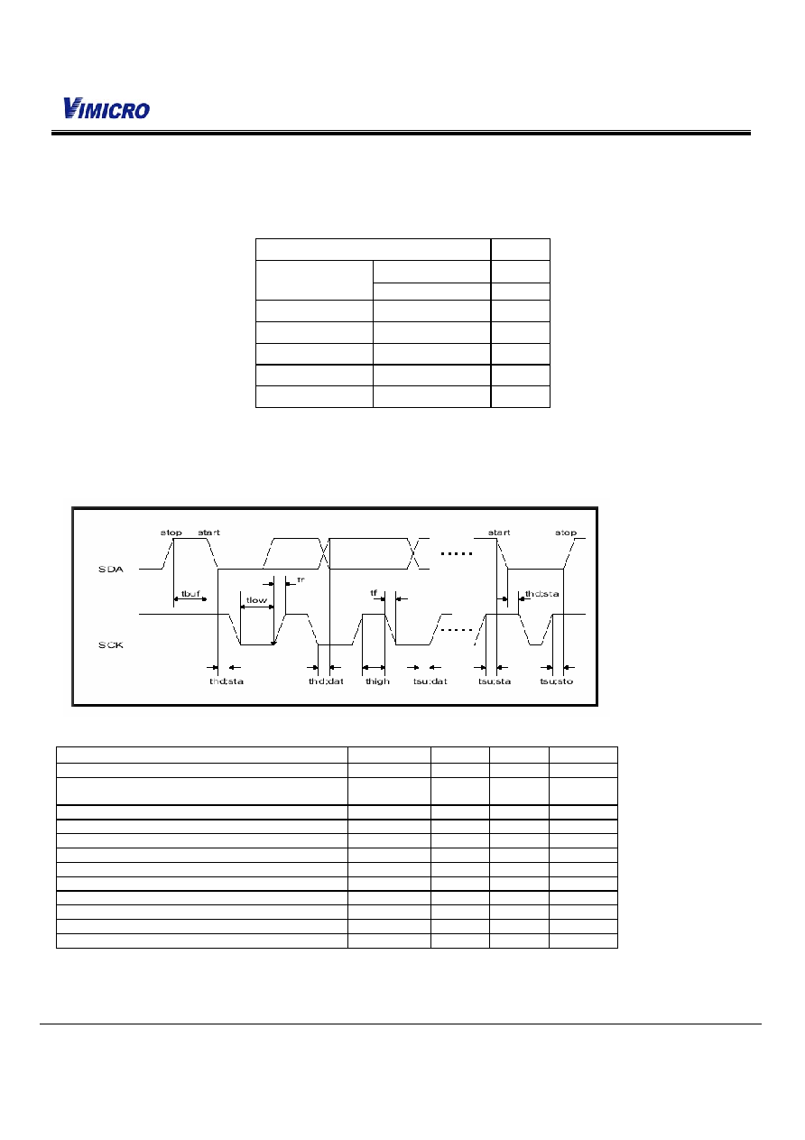
6. Appendix
F
IGURE
9. S
ERIAL
B
US
T
IMING
D
IAGRAM
Parameter Symbol
Min
Max.
Unit
SCK clock frequency
f
sck
0
100
KHz
Time that I
2
C bus must be free before a new
transmission can start
t
buf
4.7
-
us
Hold time for a START
t
hd
;S
ta
4.0
- us
LOW period of SCK
t
low
4.7
-
us
HIGH period of SCK
t
high
4.0
-
us
Setup time for START
t
su
;S
ta
4.7
- us
Data hold time
t
hd
;d
at
0 - us
Data setup time
t
su
;d
at
200
- ns
Rise time of both SDA and SCK
t
r
-
1
us
Fall time of both SDA and SCK
t
f
-
300
ns
Setup time for STOP
t
su
;S
tp
4.7
- us
Capacitive load of each bus lines (SDA, SCK)
C
b
-
-
pf
TABLE 7. S
ERIAL
B
US
T
IMING
T
ABLE
Lead Count
48
D1
7
Body Size
E1 7
Stand-Off
A1
0.1
Body Thickness
A2
1.4
Lead Width
b
0.2
Lead Thickness
c
0.127
Lead Pitch
e
0.5