Pr
eli
mi
na
ry
FEATURES
High Voltage Operation : V
DS
=50V
High Gain: 16dB(typ.) at P
out
=39dBm(Avg.)
High Efficiency: 35%(typ.) at P
out
=39dBm(Avg.)
Broad Frequency Range : 2100 to 2200MHz
Proven Reliability
DESCRIPTION
The EGN21A045IV is a 45 Watt GaN-HEMT that offers high efficiency,
high gain, ease of matching, greater consistency and broad bandwidth
for high power L-band amplifiers with 50V operation. This device is
targeted for high voltage, low current operation in digitally modulated
base station applications - ideally suited for W-CDMA base station
amplifiers and other HPA designs while offering ease of use.
ABSOLUTE MAXIMUM RATINGS
Item Symbol Condition Rating Unit
Drain-Source Voltage V
DS
120 V
Gate-Source Voltage V
GS
T
c
=25
o
C -5 V
Total Power Dissipation P
t
112 W
Storage Temperature T
stg
-65 to +175
o
C
Channel Temperature T
ch
250
o
C
ELECTRICAL CHARACTERISTICS (Case Temperature Tc=25
o
C)
Item Symbol Condition Limit Unit
Min. Typ. Max.
Pinch-Off Voltage V
p
V
DS
=50V I
DS
=18mA -1.0 -2.0 -3.5 V
Gate-Drain Breakdown Voltage V
GDO
I
GS
=- 9.0 mA
- -350 - V
3rd Order Inter modulation Distortion IM
3
V
DS
=50V - -32 - dBc
Power Gain G
p
I
DS(DC)
=250mA 15.0 16.0 - dB
Drain Efficiency
d
P
out
=39dBm(Avg.) - 35 - %
Note 1
Thermal Resistance R
th
Channel to Case - 1.8 2.0
o
C/W
Note 1 : IM3 and Gain test condition as follows:
IM3 & Gain : fo=2.135GHz, f1=2.145GHz W-CDMA(3GPP3.4 12-00) BS-1 64ch
67% clipping modulation(Peak/Avg. = 8.5dB@0.01% Probability(CCDF)) measured
over 3.84MHz at fo-10MHz and fI+10MHz.
Edition 1.0
June 2005
1
RECOMMENDED OPERATING CONDITION(Case Temperature Tc= 25
o
C)
Item Symbol Condition Limit Unit
DC Input Voltage V
DS
50 V
Forward Gate Current I
GF
R
G
=10
<9.7
mA
Reverse Gate Current I
GR
R
G
=10
>-3.6
mA
Channel Temperature T
ch
200
o
C
EGN21A045IV
High Voltage - High Power GaN-HEMT
Preliminary
Eudyna GaN-HEMT 45W

Pr
eli
mi
na
ry
2
EGN21A045IV
High Voltage - High Power GaN-HEMT
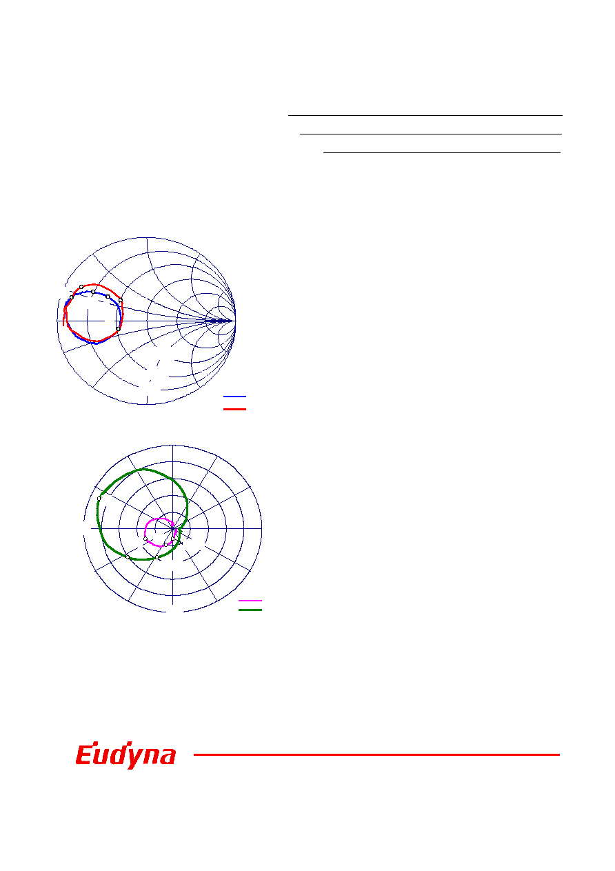
Output Power vs. Frequency
V
DS
=50V, I
DS
=250mA
2-tone IMD vs. Output Power
V
DS
=50V, f
1
=2.135GHz, f
2
=2.145GHz, 10MHz Spacing
2-tone IMD vs. Tone Spacing, V
DS
=50V, I
DS
=250mA
P
out
=39dBm(average) Center Frequency=2.14GHz
Output Power and Drain Efficiency vs. Input Power
V
DS
=50V, I
DS
=250mA, f=2.14GHz
Dr
ain Efficien
cy [%]
36
38
40
42
44
46
48
2.04 2.06 2.08 2.1 2.12 2.14 2.16 2.18 2.2 2.22 2.24
Frequency [GHz]
Output Powe
r [dBm]
Pin=21dBm
Pin=23dBm
Pin=25dBm
Pin=27dBm
Pin=29dBm
Pin=31dBm
Pin=33dBm
Pin=35dBm
-50
-45
-40
-35
-30
-25
-20
24 26 28 30 32 34 36 38 40 42 44
Output Power(average) [dBm]
IM3 [dBc]
125mA
250mA
375mA
500mA
-55
-50
-45
-40
-35
-30
-25
-20
2-tone Spacing [MHz]
IMD [dBc]
IM3 lower
IM3 upper
IM5 lower
IM5 upper
IM7 lower
IM7 upper
0.1
1.0
10
28
30
32
34
36
38
40
42
44
46
48
10 12 14 16 18 20 22 24 26 28 30 32 34 36
Input Power [dBm]
Output Powe
r [dBm]
0
10
20
30
40
50
60
70
80
90
100
Drain
Effi.
Output
Power

Pr
eli
mi
na
ry
3
EGN21A045IV
High Voltage - High Power GaN-HEMT
2-Carrier IMD, Drain Efficiency and Power Gain vs. Output Power
V
DS
=50V, I
DS
=250mA, f
1
=2.135GHz, f
2
=2.145GHz(10MHz Spacing)
Peak/Avg. = 8.5dB@0.01% Probability(CCDF)
2-Carrier ACLR, Drain Efficiency and Power Gain
vs. Output Power with DPD Operation (note
V
DS
=50V, I
DS
=250mA
f
1
=2.1375GHz, f
2
=2.1425GHz(5MHz Spacing)
Peak/Avg. = 6.5dB@0.01% Probability(CCDF);
Single Carrier Signal
Note) Digital Predistortion evaluation test system:
PMC-Sierra PALADIN-15 DPD chip-set
Dr
ain Efficien
cy [%], Pow
e
r
G
a
in
[d
B]
Output Power [dBm]
ACLR(5MHz offset) [dBc]
Dr
ain Efficien
cy [%], Pow
e
r
G
a
in
[d
B]
10
dB
/d
iv
2-carrier Spectrum with DPD Operation
DPD-OFF
DPD-ON
Center Frequency=2.14GHz
5MHz/div
Pave=39dBm
-60
-55
-50
-45
-40
-35
-30
-25
-20
-15
-10
24
26
28
30
32
34
36
38
40
42
44
Output Power [dBm]
IMD [dBc]
0
5
10
15
20
25
30
35
40
45
50
Drain
Effi.
IM3
Power
Gain
IM5
IM7
-60
-55
-50
-45
-40
-35
-30
-25
-20
-15
-10
30
32
34
36
38
40
42
0
5
10
15
20
25
30
35
40
45
50
Drain
Effi.
ACLR
DPD-OFF
Power
Gain
ACLR
DPD-ON