 | –≠–ª–µ–∫—Ç—Ä–æ–Ω–Ω—ã–π –∫–æ–º–ø–æ–Ω–µ–Ω—Ç: FLC087XP | –°–∫–∞—á–∞—Ç—å:  PDF PDF  ZIP ZIP |
1
Edition 1.3
July 1999
FLC087XP
GaAs FET & HEMT Chips
Item
Saturated Drain Current
Transconductance
Pinch-off Voltage
Gate Source Breakdown Voltage
Power-added Efficiency
Output Power at 1dB
Gain Compression Point
Power Gain at 1dB
Gain Compression Point
Symbol
IDSS
-
300
450
75
150
-
-1.0
-2.0
-3.5
-5
-
-
6.0
7.0
-
-
31.5
-
27.5
28.5
-
VDS = 5V, IDS = 15mA
VDS = 5V, IDS = 200mA
VDS = 5V, VGS = 0V
IGS = -15µA
VDS = 10V
IDS 0.6IDSS
f = 8GHz
mA
mS
V
dB
%
dBm
V
gm
Vp
VGSO
P1dB
G1dB
add
Test Conditions
Unit
Limit
Typ.
Max.
Min.
ELECTRICAL CHARACTERISTICS (Ambient Temperature Ta=25∞C)
Note: RF parameter sample size 10pcs. criteria (accept/reject)=(2/3)
Channel to Case
-
25
36
∞C/W
Thermal Resistance
Rth
The chip must be enclosed in a hermetically sealed environment for optimum performance and reliability.
DESCRIPTION
The FLC087XP chip is a power GaAs FET that is designed for general
purpose applications in the C-Band frequency range as it provides
superior power, gain, and efficiency.
Fujitsu's stringent Quality Assurance Program assures the
highest reliability and consistent performance.
FEATURES
∑ High Output Power: P1dB = 28.5dBm(Typ.)
∑ High Gain: G1dB = 7.0dB(Typ.)
∑ High PAE: add = 31.5%(Typ.)
∑ Proven Reliability
Item
Drain-Source Voltage
Gate-Source Voltage
Total Power Dissipation
Storage Temperature
Channel Temperature
Symbol
VDS
VGS
15
-5
4.16
-65 to +175
175
Tc = 25∞C
V
V
W
∞C
∞C
Ptot
Tstg
Tch
Condition
Unit
Rating
ABSOLUTE MAXIMUM RATING (Ambient Temperature Ta=25∞C)
Fujitsu recommends the following conditions for the reliable operation of GaAs FETs:
1. The drain-source operating voltage (VDS) should not exceed 10 volts.
2. The forward and reverse gate currents should not exceed 4.8 and -0.5 mA respectively with
gate resistance of 400.
3. The operating channel temperature (Tch) should not exceed 145∞C.
Drain
Gate
Source
Source

2
FLC087XP
GaAs FET & HEMT Chips
POWER DERATING CURVE
DRAIN CURRENT vs. DRAIN-SOURCE VOLTAGE
3
4
5
2
1
0
50
100
150
200
2
4
6
8
10
Case Temperature (∞C)
Drain-Source Voltage (V)
Total Power Dissipation (W)
300
200
100
Drain Current (mA)
VGS =0V
-0.5V
-1.5V
-2.0V
-1.0V
OUTPUT POWER vs. INPUT POWER
P1dB & add vs. VDS
VDS=10V
IDS0.6IDSS
f=8GHz
IDS0.6IDSS
f=4GHz
f=4GHz
8GHz
8GHz
add
Pout
add
P1dB
26
28
30
22
12 14
16
16
18
18
20
30
40
20
10
20 22
24
24
Input Power (dBm)
Output Power (dBm)
29
30
27
8
9
10
26
28
Drain-Source Voltage (V)
P
1dB
(dbm)
add (%)
30
20
10
add (%)

3
FLC087XP
GaAs FET & HEMT Chips
S-PARAMETERS
VDS = 10V, IDS = 200mA
FREQUENCY
S11
S21
S12
S22
(MHZ)
MAG
ANG
MAG
ANG
MAG
ANG
MAG
ANG
100
.998
-11.7
9.704
172.7
.006
83.8
.510
-4.7
500
.965
-54.6
8.567
145.8
.026
61.3
.467
-21.1
1000
.914
-92.8
6.593
121.3
.039
42.4
.399
-34.2
1500
.883
-116.8
5.088
104.7
.046
31.3
.355
-42.2
2000
.866
-132.5
4.067
92.4
.048
24.5
.332
-48.2
2500
.857
-143.5
3.363
82.4
.050
20.0
.323
-53.7
3000
.852
-151.7
2.856
73.7
.051
16.9
.320
-59.0
3500
.848
-158.1
2.478
65.9
.051
14.6
.323
-64.3
4000
.846
-163.4
2.186
58.6
.052
12.9
.330
-69.7
4500
.845
-167.9
1.954
51.8
.052
11.5
.338
-74.9
5000
.845
-171.8
1.765
45.2
.052
10.5
.349
-80.2
5500
.845
-175.3
1.608
38.9
.052
9.6
.362
-85.3
6000
.845
-178.4
1.476
32.7
.053
8.9
.375
-90.4
6500
.845
178.7
1.362
26.7
.053
8.4
.390
-95.3
7000
.846
176.1
1.264
20.8
.053
8.0
.406
-100.2
7500
.847
173.6
1.177
15.0
.053
7.6
.422
-105.0
8000
.847
171.2
1.099
9.3
.053
7.3
.439
-109.6
8500
.848
169.0
1.030
3.7
.053
7.1
.456
-114.2
9000
.849
166.8
.967
-1.9
.053
7.0
.474
-118.7
9500
.850
164.7
.909
-7.4
.053
6.9
.492
-123.1
10000
.852
162.7
.856
-12.8
.054
6.8
.511
-127.5
10500
.853
160.8
.806
-18.1
.054
6.7
.529
-131.7
11000
.854
158.9
.760
-23.4
.054
6.7
.548
-135.9
11500
.855
157.1
.716
-28.7
.054
6.7
.567
-140.0
12000
.857
155.3
.675
-33.9
.055
6.6
.585
-144.0
NOTE:*
The data includes bonding wires.
n: number of wires
Gate
n=1 (0.3mm length, 25µm Dia Au wire)
Drain n=1 (0.3mm length, 25µm Dia Au wire)
Source n=4 (0.3mm length, 25µm Dia Au wire)
Download S-Parameters, click here

For further information please contact:
FUJITSU COMPOUND SEMICONDUCTOR, INC.
2355 Zanker Rd.
San Jose, CA 95131-1138, U.S.A.
Phone: (408) 232-9500
FAX: (408) 428-9111
www.fcsi.fujitsu.com
FUJITSU MICROELECTRONICS, LTD.
Compound Semiconductor Division
Network House
Norreys Drive
Maidenhead, Berkshire SL6 4FJ
Phone:+44 (0)1628 504800
FAX:+44 (0)1628 504888
Fujitsu Limited reserves the right to change products and specifications without notice.
The information does not convey any license under rights of Fujitsu Limited or others.
© 1998 FUJITSU COMPOUND SEMICONDUCTOR, INC.
Printed in U.S.A. FCSI0598M200
Fujitsu Compound Semiconductor Products contain gallium arsenide
(GaAs) which can be hazardous to the human body and the environment.
For safety, observe the following procedures:
CAUTION
∑ Do not put these products into the mouth.
∑ Do not alter the form of this product into a gas, powder, or liquid
through burning, crushing, or chemical processing as these by-products
are dangerous to the human body if inhaled, ingested, or swallowed.
∑ Observe government laws and company regulations when discarding this
product. This product must be discarded in accordance with methods
specified by applicable hazardous waste procedures.
4
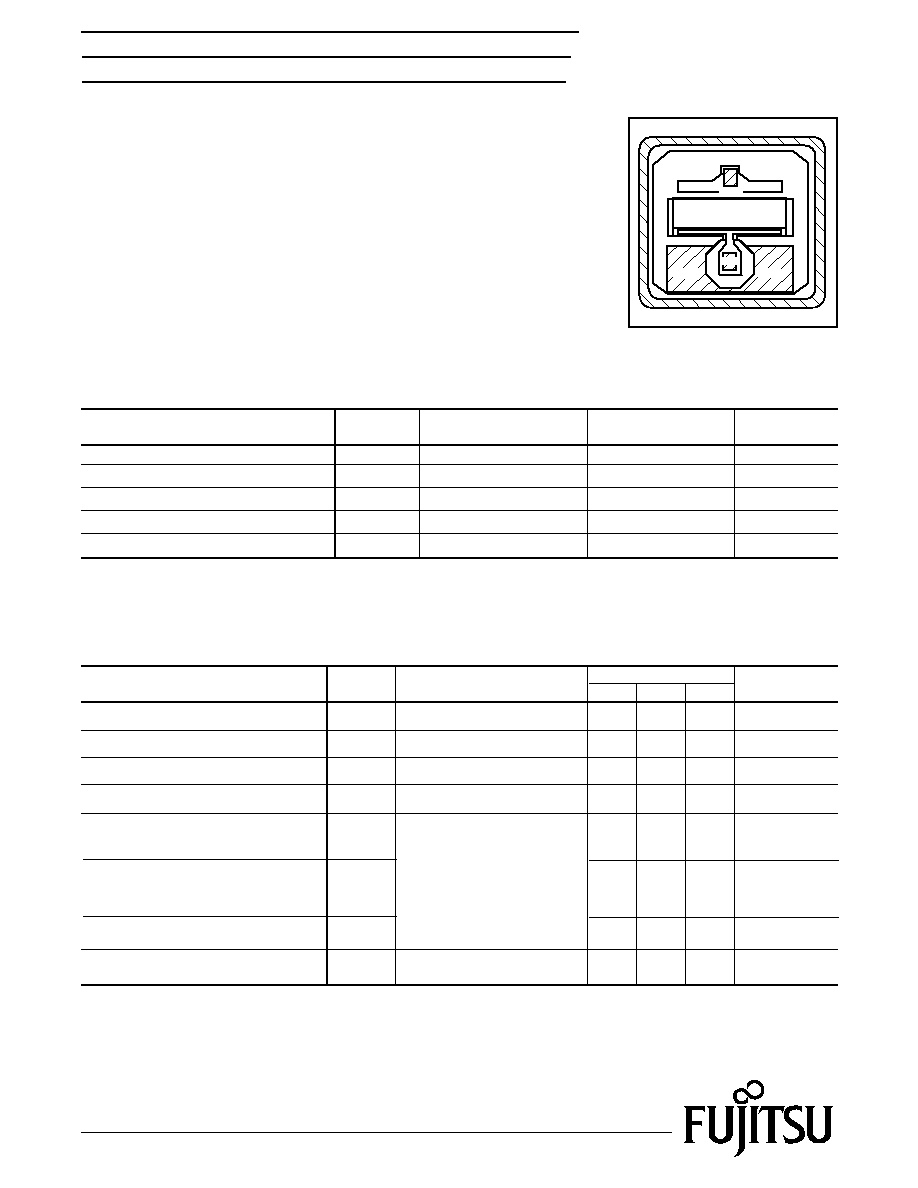
CHIP OUTLINE
(Unit: µm)
Source electrodes are electrically
insulated from the bottom of the
chip (PHS)
Die Thickness: 60±20µm
610
±
30
500
65
155
60
660±30
Drain
70
170
Gate
Source
Source
550
50
155
FLC087XP
GaAs FET & HEMT Chips