1
Edition 1.0
February 2000
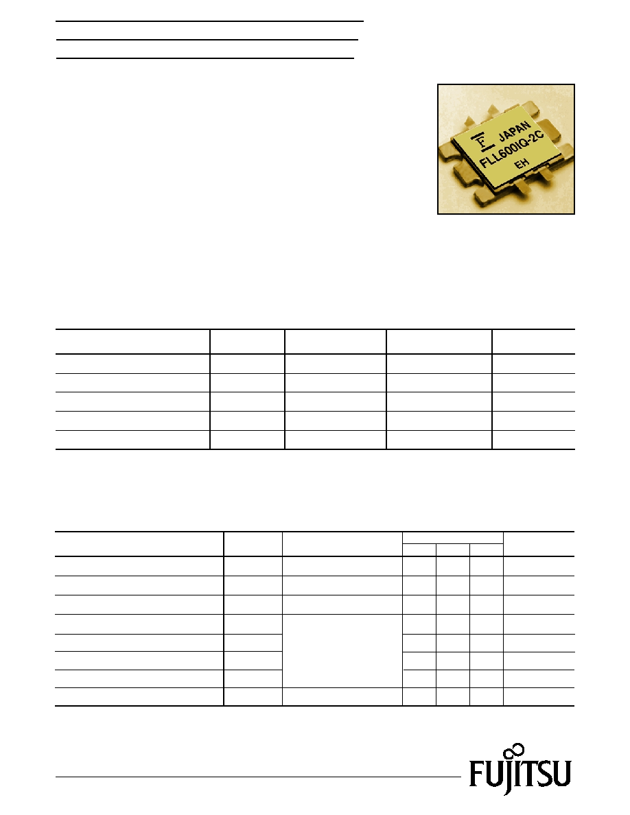
FLL600IQ-2C
L-Band High Power GaAs FET
DESCRIPTION
The FLL600IQ-2C is a 60 Watt GaAs FET that employs a push-pull design that
offers ease of matching, greater consistency and a broader bandwidth for high
power L-band amplifiers. This product is targeted to reduce the size and
complexity of highly linear, high power base station transmitting amplifiers.
This new product is uniquely suited for use in W-CDMA and IMT 2000 base
station amplifiers as it offers high gain, long term reliability and ease of use.
FEATURES
∑ Push-Pull Configuration
∑ High Power Output: 60W (Typ.)
∑ High PAE: 51% (Typ.)
∑ Broad Frequency Range: 2100 to 2200 MHz.
∑ Suitable for class AB operation.
APPLICATIONS
∑ Solid State Base-Station Power Amplifier.
∑ W-CDMA and IMT 2000 Communication Systems.
Item
Drain Current
Pinch-Off Voltage
Gate-Source Breakdown Voltage
Output Power
Linear Gain
Power-Added Efficiency
Thermal Resistance
Symbol
I
DSS
V
GSO
-
6
-
-0.1
-0.3
-0.5
-5
-
-
47.0
48.0
-
11.0
12.0
-
-
51
-
-
0.8
1.2
V
DS
= 5V, V
GS
= 0V
V
DS
= 5V, I
DS
= 151mA
I
GS
= -1.51mA
Channel to Case
V
DS
= 12V
f = 2.17 GHz
I
DS
= 1.5A
Pin = 39dBm
A
V
dB
dBm
V
∞C/W
%
V
p
P
out
GL
add
Drain Current
-
9
13
A
I
DSR
R
th
Conditions
Unit
Limits
Typ.
Max.
Min.
ELECTRICAL CHARACTERISTICS (Case Temperature Tc=25∞C)
CASE STYLE: IU
Item
Drain-Source Voltage
Gate-Source Voltage
Total Power Dissipation
Storage Temperature
Channel Temperature
Symbol
V
DS
Tc = 25∞C
V
V
W
∞C
∞C
V
GS
P
T
T
stg
T
ch
Condition
125
-65 to +175
+175
-5
15
Rating
Unit
ABSOLUTE MAXIMUM RATINGS (Ambient Temperature Ta=25∞C)
Fujitsu recommends the following conditions for the reliable operation of GaAs FETs:
1. The drain-source operating voltage (VDS) should not exceed 12 volts.
2. The forward and reverse gate currents should not exceed 117 and -35.4 mA respectively with
gate resistance of 10.
3. The operating channel temperature (Tch) should not exceed 145∞C.

2
FLL600IQ-2C
L-Band High Power GaAs FET
-50
ACP vs. OUTPUT POWER
35
37
36
38
39
40
41
42
43
44
34
36
35
37
38
39
40
41
42
43
44
-55
-60
-65
-45
-40
-35
-30
-25
Output Power (dBm)
ACP (dBc)
VDS = 12V
IDS = 1.5A
fo = 2.14GHz
W-CDMA Single Signal
VDS = 12V
IDS = 1.5A
Wide Band Tuned
OUTPUT POWER vs. FREQUENCY
1.99 2.02
2.14
2.20 2.23
2.05
2.08 2.11
2.17
2.26 2.29 2.32
34dBm
36dBm
38dBm
40dBm
32dBm
30dBm
28dBm
26dBm
24dBm
22dBm
34
36
38
40
42
44
46
48
50
Frequency (GHz)
-5MHz
+5MHz
-10MHz
+10MHz
-50
IMD vs. OUTPUT POWER
-55
-60
-65
-45
-40
-35
-30
Output Power (dBm)
IMD (dBc)
VDS = 12V
IDS = 1.5A
f = 2.14GHz
f = 1MHz
Wide Band Tuned
+IM3
+IM5
OUTPUT POWER & add vs. INPUT POWER
VDS =12V
IDS = 1.5A
f = 2.17GHz
Wide Band Tuned
20
24
28
32
36
40
Input Power (dBm)
Output Power (dBm)
Output Power (dBm)
add
Pout
add (%)
40
42
44
46
48
28
30
32
34
36
38
50
40
20
30
10
4
For further information please contact:
FUJITSU COMPOUND SEMICONDUCTOR, INC.
2355 Zanker Rd.
San Jose, CA 95131-1138, U.S.A.
Phone: (408) 232-9500
FAX: (408) 428-9111
www.fcsi.fujitsu.com
FME, QDD (European Sales Office)
Fujitsu Microelectronics Europe GmbH
Quantum Devices Division
Network House
Norreys Drive
Maidenhead, Berkshire SL6 4FJ
Phone:+44 (0)1628 504800
FAX:+44 (0)1628 504888
Fujitsu Limited reserves the right to change products and specifications without notice.
The information does not convey any license under rights of Fujitsu Limited or others.
© 1999 FUJITSU COMPOUND SEMICONDUCTOR, INC.
Printed in U.S.A. FCSI1199M200
Fujitsu Compound Semiconductor Products contain gallium arsenide
(GaAs) which can be hazardous to the human body and the environment.
For safety, observe the following procedures:
CAUTION
∑ Do not put these products into the mouth.
∑ Do not alter the form of this product into a gas, powder, or liquid
through burning, crushing, or chemical processing as these by-products
are dangerous to the human body if inhaled, ingested, or swallowed.
∑ Observe government laws and company regulations when discarding this
product. This product must be discarded in accordance with methods
specified by applicable hazardous waste procedures.
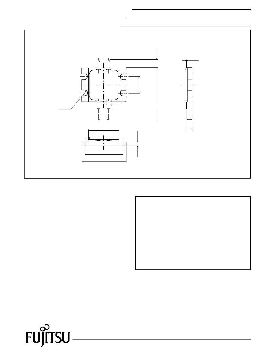
FLL600IQ-2C
L-Band High Power GaAs FET
Case Style "IQ"
Unit: mm (inches)
8.0
(0.315)
1.9
(0.075)
2.5 MIN.
2.5 MIN.
17.4
(0.685)
4-R1.3
(0.051)
16.4
(0.646)
±0.2
±0.15
6.0
(0.236)
±0.2
20.4
(0.803)
±0.2
24.0
(0.945)
±0.2
±
0.2
±
0.2
2.0
(0.079)
1
2
5
4
3
1, 2: Gate
3: Source
4, 5: Drain
±0.13
2.4
(0.094)
4.4 Max.
0.1
(0.004)
