
1
Edition 1.1
October 2001
Item
Drain-Source Voltage
Gate-Source Voltage
Total Power Dissipation
Storage Temperature
Channel Temperature
Symbol
V
DS
Tc = 25
∞
C
V
V
W
∞
C
∞
C
V
GS
P
T
T
stg
T
ch
Condition
136
-65 to +175
+175
-5
15
Rating
Unit
ABSOLUTE MAXIMUM RATINGS (Ambient Temperature Ta=25
∞
C)
Fujitsu recommends the following conditions for the reliable operation of GaAs FETs:
1. The drain-source operating voltage (VDS) should not exceed 12 volts.
2. The forward and reverse gate currents should not exceed 176 and -51.8 mA respectively with
gate resistance of 5
.
3. The operating channel temperature (Tch) should not exceed 145
∞
C.
FEATURES
∑ Push-Pull Configuration
∑ High Power Output: 80W
∑ High PAE: 45%.
∑ Excellent Linearity
∑ Suitable for class AB operation.
∑ Hermetically Sealed Package
DESCRIPTION
The FLL810IQ-4C is an 80 Watt GaAs FET that employs a push-pull design
which offers excellent linearity, ease of matching, and greater consistency in
covering the frequency band of 3.5 to 3.7 GHz. This new product is uniquely
suited for use in WLL applications as it offers high gain, long term reliability and
ease of use.
FLL810IQ-4C
L-Band High Power GaAs FET
Item
Symbol
V
DS
= 12V
f = 3.6 GHz
I
DS
= 5.0A
Pin = 43.0dBm
Gate-Source Breakdown Voltage
V
GSO
-5
-
-
I
GS
= -2.2mA
V
Pinch-Off Voltage
-0.1
-0.3
-0.5
V
DS
= 5V, I
DS
= 220mA
V
V
p
Drain Current
-
8
-
V
DS
= 5V, V
GS
= 0V
A
I
DSS
Drain Current
-
11.5
15.0
A
I
DSR
Output Power
48.0
49.0
-
dBm
P
out
Linear Gain (Note 1)
8.5
9.5
-
dB
GL
Power-Added Efficiency
-
45
-
%
add
Thermal Resistance
-
0.8
1.1
Channel to Case
∞
C/W
R
th
Conditions
Unit
Limits
Typ.
Max.
Min.
ELECTRICAL CHARACTERISTICS (Case Temperature Tc=25
∞
C)
CASE STYLE: IQ
Note 1: The condition for GL is the same as Pout except Pin = 28.0dBm.
2
FLL810IQ-4C
L-Band High Power GaAs FET
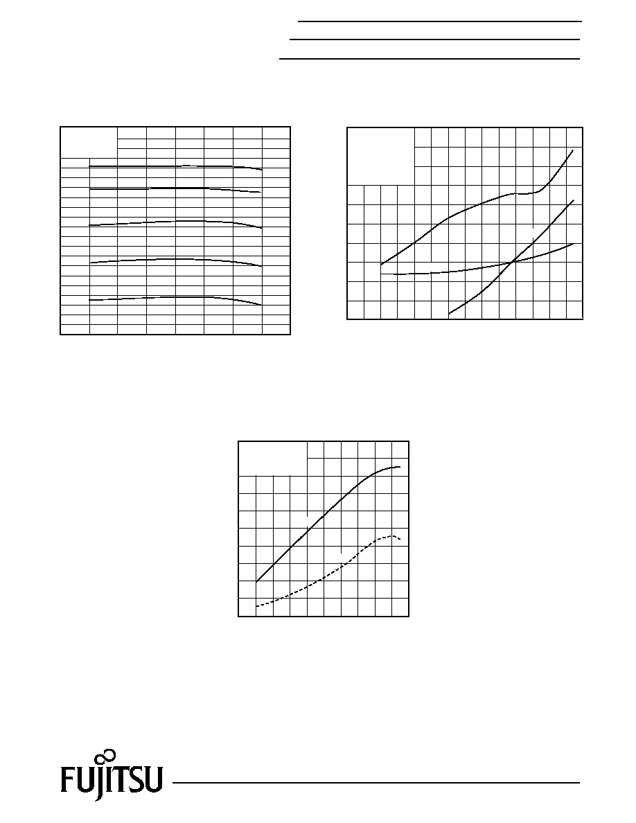
OUTPUT POWER &
add vs. INPUT POWER
34
36
40
38
44
42
46
48
26 28
32
30
34
36 38
40
42
Input Power (dBm)
VDS = 12V,
IDS(DC) = 5A,
f = 3.6GHz
Output Power (dBm)
10
20
30
40
50
add
(%)
add
Pout
IM3
IM5
IDS(RF)
IMD & IDS(RF) vs. TOTAL OUTPUT POWER
-56
-60
-52
-48
-44
-40
-36
-32
-28
-24
2
4
6
8
10
12
14
16
18
34
33
35 36
37 38 39 40 41 42 43 44 45
Total Output Power (dBm)
VDS = 12V,
IDS(DC) = 5A,
fo = 3.6GHz,
f1 = 3.61GHz
IMD (dBc)
IDS(RF) (A)
34
36
38
40
42
44
46
48
50
3.50
3.45
3.55
3.60
3.65
3.70
3.75
Frequency (GHz)
Output Power (dBm)
OUTPUT POWER vs. FREQUENCY
38dBm
43dBm
34dBm
30dBm
26dBm
VDS = 12V,
IDS(DC) = 5A

3
FLL810IQ-4C
L-Band High Power GaAs FET
S-PARAMETERS
VDS = 12V, IDS = 2500mA
FREQUENCY
S11
S21
S12
S22
(MHZ)
MAG
ANG
MAG
ANG
MAG
ANG
MAG
ANG
2500
.499
-103.9
1.973
-113.4
.017
-111.7
.796
152.9
2600
.617
-120.1
1.880
-125.9
.017
-134.2
.773
151.8
2700
.703
-131.7
1.735
-142.2
.016
-149.9
.752
150.1
2800
.761
-141.4
1.784
-153.8
.016
-167.5
.729
149.5
2900
.793
-148.6
1.689
-163.9
.017
-176.4
.714
148.0
3000
.801
-155.5
1.803
-178.8
.017
161.0
.678
146.2
3100
.783
-162.8
1.949
171.0
.019
136.6
.656
143.9
3200
.747
-169.1
2.087
154.5
.021
119.4
.604
140.8
3300
.644
-176.8
2.398
136.9
.024
94.7
.566
138.8
3400
.492
178.6
2.627
116.1
.031
80.3
.506
137.6
3500
.315
-166.2
2.798
88.0
.036
48.3
.468
143.3
3600
.397
-130.1
2.612
59.6
.034
15.7
.504
148.1
3700
.603
-128.8
2.173
33.1
.031
-8.8
.558
145.3
3800
.743
-135.6
1.814
13.3
.024
-33.0
.580
136.4
3900
.825
-143.0
1.493
-5.2
.022
-47.8
.559
125.9
4000
.878
-148.0
1.222
-20.4
.019
-59.2
.535
113.4
4100
.910
-152.6
.999
-34.6
.019
-67.0
.483
97.7
4200
.937
-156.1
.849
-46.9
.017
-76.4
.418
78.8
4300
.949
-159.8
.735
-55.8
.018
-86.6
.376
53.9
4400
.953
-162.7
.681
-67.5
.018
-96.7
.343
18.9
4500
.956
-165.1
.666
-82.1
.020
-107.9
.386
-17.4
Note: This S-Parameter data shows measurements performed on a single-ended push-pull FET. These parameters should be used
to determine the calculated Push-Pull S-Parameter amplifier designs.
Download S-Parameters, click here

4
For further information please contact:
FUJITSU COMPOUND SEMICONDUCTOR, INC.
2355 Zanker Rd.
San Jose, CA 95131-1138, U.S.A.
Phone: (408) 232-9500
FAX: (408) 428-9111
www.fcsi.fujitsu.com
FUJITSU QUANTUM DEVICES EUROPE LTD.
Network House
Norreys Drive
Maidenhead, Berkshire SL6 4FJ
Phone:+44 (0)1628 504800
FAX:+44 (0)1628 504888
Fujitsu Limited reserves the right to change products and specifications without notice.
The information does not convey any license under rights of Fujitsu Limited or others.
© 2001 FUJITSU COMPOUND SEMICONDUCTOR, INC.
Printed in U.S.A. FCSI05019M200
Fujitsu Compound Semiconductor Products contain gallium arsenide
(GaAs) which can be hazardous to the human body and the environment.
For safety, observe the following procedures:
CAUTION
∑ Do not put these products into the mouth.
∑ Do not alter the form of this product into a gas, powder, or liquid
through burning, crushing, or chemical processing as these by-products
are dangerous to the human body if inhaled, ingested, or swallowed.
∑ Observe government laws and company regulations when discarding this
product. This product must be discarded in accordance with methods
specified by applicable hazardous waste procedures.
FLL810IQ-4C
L-Band High Power GaAs FET
Case Style "IQ"
15.5±
0.2
2.4±0.15
4-0.1
1.9±
0.2
5.5 Max.
14.9±0.2
8.0±
0.15
2.5 MIN.
2.5 MIN.
4-R1.3±0.2
6.0
4-2.6±
0.2
17.4±
0.2
4-2.0
1
2
5
4
3
6
24±0.35
20.4±0.2
45∞
Unit: mm (inches)
1, 2: Gate
3:
Source
4, 5: Drain