
1
Edition 1.4
August 2004
FLM1011-6F
X, Ku-Band Internally Matched FET
Item
Drain-Source Voltage
Gate-Source Voltage
Total Power Dissipation
Storage Temperature
Channel Temperature
Symbol
VDS
VGS
15
-5
31.2
-65 to +175
175
Tc = 25∞C
V
V
W
∞C
∞C
PT
Tstg
Tch
Condition
Unit
Rating
ABSOLUTE MAXIMUM RATING (Ambient Temperature Ta=25
∞C)
Fujitsu recommends the following conditions for the reliable operation of GaAs FETs:
1. The drain-source operating voltage (VDS) should not exceed 10 volts.
2. The forward and reverse gate currents should not exceed 26.0 and -2.8 mA respectively with
gate resistance of 100
.
Item
Saturated Drain Current
Transconductance
Pinch-off Voltage
Gate Source Breakdown Voltage
Output Power at 1dB G.C.P.
Power Gain at 1dB G.C.P.
Symbol
IDSS
-
2800
4200
-0.5
-1.5
-3.0
36.5
37.5
-
6.5
7.5
-
VDS = 5V, IDS = 120mA
VDS = 5V, IDS = 1800mA
VDS = 5V, VGS = 0V
IGS = -120µA
VDS = 10V,
IDS = 0.6 IDSS(Typ.),
f = 10.7 ~ 11.7 GHz,
ZS = ZL = 50
mA
V
-
2350
-
mS
-5
-
-
V
dB
dBm
gm
Vp
VGSO
P1dB
G1dB
Drain Current
-
1800
2100
mA
Idsr
Power-Added Efficiency
-
28
-
%
add
Gain Flatness
-
-
±0.6
dB
G
Thermal Resistance
Channel to Case
-
4.0
4.5
∞C/W
CASE STYLE: IA
Rth
3rd Order Intermodulation
Distortion
f = 11.7GHz,
f = 10MHz
2-Tone Test
Pout = 25dBm S.C.L.
-42
-45
-
dBc
IM3
Test Conditions
Unit
Limit
Typ.
Max.
Min.
ELECTRICAL CHARACTERISTICS (Ambient Temperature Ta=25
∞C)
G.C.P.: Gain Compression Point, S.C.L.: Single Carrier Level
DESCRIPTION
The FLM1011-6F is a power GaAs FET that is internally matched for
standard communication bands to provide optimum power and gain in a
50 ohm system.
Eudyna's stringent Quality Assurance Program assures the highest
reliability and consistent performance.
FEATURES
∑ High Output Power: P1dB = 37.5dBm (Typ.)
∑ High Gain: G1dB = 7.5dB (Typ.)
∑ High PAE:
add = 28% (Typ.)
∑ Low IM3 = -45dBc@Po = 25dBm
∑ Broad Band: 10.7 ~ 11.7GHz
∑ Impedance Matched Zin/Zout = 50
∑ Hermetically Sealed

2
FLM1011-6F
X, Ku-Band Internally Matched FET
POWER DERATING CURVE
50
0
100
150
200
Case Temperature (
∞C)
40
30
20
10
Total Power Dissipation (W)
OUTPUT POWER & IM3 vs. INPUT POWER
VDS=10V
f1 = 11.7 GHz
f2 = 11.71 GHz
2-tone test
15
19
17
21
23
25
Input Power (S.C.L.) (dBm)
S.C.L.: Single Carrier Level
Output Power (S.C.L.) (dBc)
-20
-30
-40
-50
28
26
24
30
32
22
IM
3
(dBc)
IM3
Pout
OUTPUT POWER vs. FREQUENCY
Pin=32dBm
P1dB
28dBm
26dBm
24dBm
22dBm
20dBm
10.8
11.4
11.2
11.0
11.6
Frequency (GHz)
31
33
35
37
29
27
Output Power (dBm)
OUTPUT POWER vs. INPUT POWER
26
28
30
32
34
36
38
20
22
24
26
28
30
32
20
10
30
40
Input Power (dBm)
Output Power (dBm)
add
Pout
add
(%)
VDS=10V
f = 11.2 GHz
VDS=10V
P1dB
Eudyna Devices Inc. products contain gallium arsenide
(GaAs) which can be hazardous to the human body and the environment.
For safety, observe the following procedures:
CAUTION
∑ Do not put this product into the mouth.
∑ Do not alter the form of this product into a gas, powder, or liquid
through burning, crushing, or chemical processing as these by-products
are dangerous to the human body if inhaled, ingested, or swallowed.
∑ Observe government laws and company regulations when discarding this
product. This product must be discarded in accordance with methods
specified by applicable hazardous waste procedures.
For further information please contact:
Eudyna Devices USA Inc.
2355 Zanker Rd.
San Jose, CA 95131-1138, U.S.A.
TEL: (408) 232-9500
FAX: (408) 428-9111
www.us.eudyna.com
Eudyna Devices Europe Ltd.
Network House
Norreys Drive
Maidenhead, Berkshire SL6 4FJ
United Kingdom
TEL: +44 (0) 1628 504800
FAX: +44 (0) 1628 504888
Eudyna Devices Asia Pte Ltd.
Hong Kong Branch
Rm. 1101, Ocean Centre, 5 Canton Rd.
Tsim Sha Tsui, Kowloon, Hong Kong
TEL: +852-2377-0227
FAX: +852-2377-3921
Eudyna Devices Inc.
Sales Division
1, Kanai-cho, Sakae-ku
Yokohama, 244-0845, Japan
TEL: +81-45-853-8156
FAX: +81-45-853-8170
Eudyna Devices Inc. reserves the right to change products and specifications
without notice. The information does not convey any license under rights of
Eudyna Devices Inc. or others.
© 2004 Eudyna Devices USA Inc.
Printed in U.S.A.
4
FLM1011-6F
X, Ku-Band Internally Matched FET
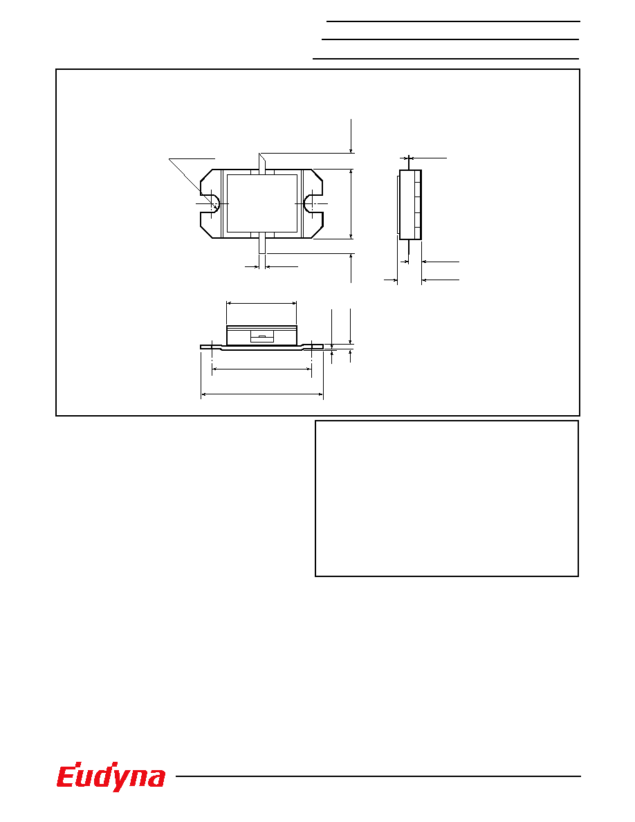
2-R 1.25
±0.15
(0.049)
0.5
(0.020)
8.1
(0.319)
13.0
±0.15
(0.512)
16.5
±0.15
(0.650)
3.2 Max.
(0.126)
1.8
±0.15
(0.071)
0.1
(0.004)
9.7
±
0.15
(0.382)
1.5 Min.
(0.059)
1.5 Min.
(0.059)
1.15
(0.045)
0.2 Max.
(0.008)
Case Style "IA"
Metal-Ceramic Hermetic Package
Unit: mm(inches)
1. Gate
2. Source (Flange)
3. Drain
4. Source (Flange)
1
2
3
4
