C-Band Internally Matched FET
FEATURES
High Output Power: P1dB=46.5dBm(Typ.)
High Gain: G1dB=8.5dB(Typ.)
High PAE:
add=36%(Typ.)
Broad Band: 5.3~5.9GHz
Impedance Matched Zin/Zout = 50
Hermetically Sealed Package
Edition 1.2
September 2004
1
FLM5359-45F
DESCRIPTION
The FLM5359-45F is a power GaAs FET that is internally matched
for standard communication bands to provide optimum power and
gain in a 50
system.
ABSOLUTE MAXIMUM RATINGS (Case Temperature Tc=25
o
C)
Item
Symbol
Unit
Drain-Source Voltage
V
DS
V
Gate-Source Voltage
V
GS
V
Total Pow er Dissipation
P
T
W
Storage Temperature
T
s tg
o
C
Channel Temperature
T
ch
o
C
RECOMMENDED OPERATING CONDITION (Case Temperature Tc=25
o
C)
Item
Symbol
Unit
DC Input Voltage
V
DS
V
Forw ard Gate Current
I
GF
mA
Reverse Gate Current
I
GR
mA
ELECTRICAL CHARACTERISTICS (Case Temperature Tc=25
o
C)
Min.
Typ.
Max.
Drain Current
I
DSS
-
16.0
-
A
Transconductance
g
m
-
8000
-
mS
Pinch-off Voltage
V
p
-1.0
-2.0
-3.5
V
Gate-Source Breakdow n Voltage
V
GSO
-5.0
-
-
V
Output Pow er at 1dB G.C.P.
P
1d B
46.0
46.5
-
dBm
Pow er Gain at 1dB G.C.P.
G
1d B
7.5
8.5
-
dB
Drain Current
I
d s r
-
8.5
10.0
A
Pow er-added Efficiency
N
ad d
-
36
-
%
Gain Flatness
G
-
-
1.4
dB
Thermal Resistance
R
th
Channel to Case
-
0.8
1.0
o
C/W
Channel Temperature Rise
T
ch
-
-
100
o
C
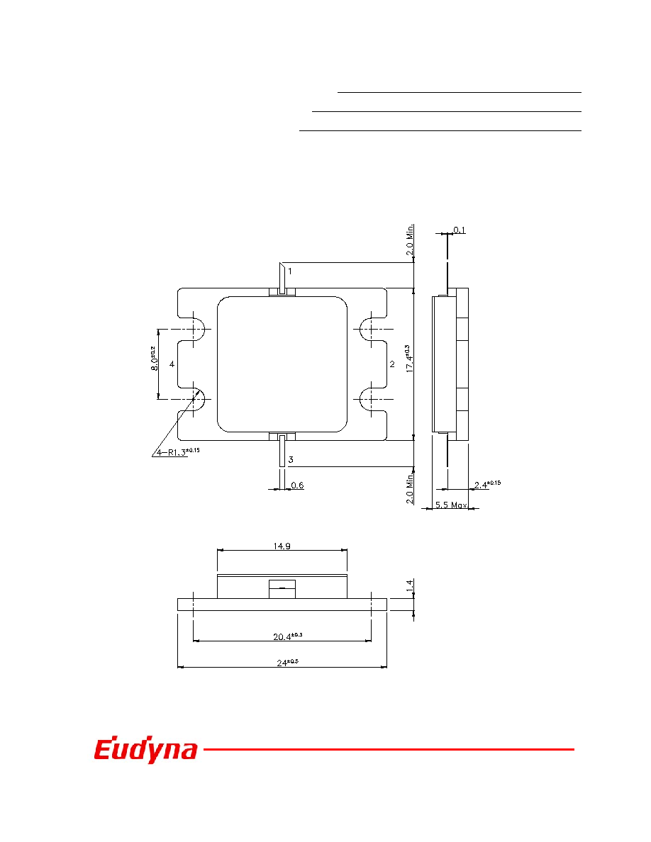
CASE STYLE : IK
G.C.P.: Gain Compression Point
ESD
Class III
2000V~
Note : Based on EIAJ ED-4701 C-111A (C=100pF, R=1.5k)
Condition
Limit
-65 to +175
175
115.4
Rating
15
-5
12
R
G
=13 ohm
107.2
R
G
=13 ohm
-23.2
Item
Symbol
Condition
Limit
I
GS
=-960uA
V
DS
=12V
I
DS
(DC)=8.0A
(typ.)
f= 5.3
~
5.9 GHz
Zs=Z
L
=50 ohm
12V x I
DS
(DC) X R
th
Unit
V
DS
=5V, V
GS
=0V
V
DS
=5V, I
DS
=8.0A
V
DS
=5V, I
DS
=960mA
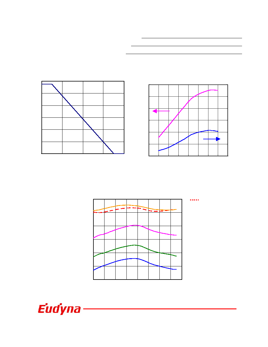
36
38
40
42
44
46
48
5.2
5.3
5.4
5.5
5.6
5.7
5.8
5.9
6.0
Frequency [GHz]
Ou
t
put
P
o
we
r
[
d
B
m
]
36
38
40
42
44
46
48
26
28
30
32
34
36
38
40
42
Input Power (dBm)
Out
put
P
o
we
r
(
d
B
m
)
0
20
40
60
80
100
120
Po
w
e
r
A
d
d
e
d
Ef
fi
c
i
e
n
c
y
(%
)
0
20
40
60
80
100
120
0
50
100
150
200
Case Temperature [ C]
Tot
a
l
P
o
w
e
r
D
i
s
s
i
pa
t
i
on [
W
]
FLM5359-45F
C-Band Internally Matched FET
2
OUTPUT POWER & POWER ADDED EFFICIENCY
vs INPUT POWER
POWER DERATING CURVE
VDS=12V, IDS=8.0A, f=5.6GHz
Pin=38dBm
P1dB
33dBm
30dBm
OUTPUT POWER vs FREQUENCY
VDS=12V, IDS=8.0A
O
28dBm

FLM5359-45F
C-Band Internally Matched FET
5
For further information please contact :
Eudyna Devices USA Inc.
2355 Zanker Rd.
San Jose, CA 95131-1138, U.S.A.
TEL: (408) 232-9500
FAX: (408) 428-9111
www.us.eudyna.com
Eudyna Devices Europe Ltd.
Network House
Norreys Drive
Maidenhead, Berkshire SL6 4FJ
United Kingdom
TEL: +44 (0) 1628 504800
FAX: +44 (0) 1628 504888
CAUTION
Eudyna Devices Inc. products contain gallium arsenide
(GaAs) which can be hazardous to the human body and the
environment. For safety, observe the following procedures:
Do not put these products into the mouth.
Do not alter the form of this product into a gas, powder, or liquid
through burning, crushing, or chemical processing as these by-
products are dangerous to the human body if inhaled, ingested, or
swallowed.
Observe government laws and company regulations when
discarding this product. This product must be discarded in
accordance with methods specified by applicable hazardous waste
procedures.
Eudyna Devices Asia Pte. Ltd.
Hong Kong Branch
Rm.1101,Ocean Centre, 5 Canton Road
Tsim Sha Tsui, Kowloon, Hong Kong
TEL: +852-2377-0227
FAX: +852-2377-3921
Eudyna Devices Inc.
1000 Kamisukiahara, showa-cho
Nakakomagun, Yamanashi
409-3883, Japan
(Kokubo Industrial Park)
TEL +81-55-275-4411
FAX +81-55-275-9461
Sales Division
1, Kanai-cho, Sakae-ku
Yokohama,244-0845,Japan
TEL +81-45-853-8156
FAX +81-45-853-8170
© 2004 Eudyna Devices USA Inc.
Printed in U.S.A.
Eudyna Devices Inc. reserves the right to change products and
specifications without notice.The information does not convey any
license under rights of Eudyna Devices Inc. or others.