1
Edition 1.2
July 1999
FSX027WF
General Purpose GaAs FET
Item
Drain-Source Voltage
Gate-Source Voltage
Total Power Dissipation
Storage Temperature
Channel Temperature
Symbol
V
V
W
∞
C
∞
C
VGS
PT
TSTG
TCH
VDS
Rating
Condition
Unit
12
-5
1.5
Tc = 25
∞
C
-65 to 175
175
ABSOLUTE MAXIMUM RATINGS (Ambient Temperature Ta = 25
∞
C)
Fujitsu recommends the following conditions for the reliable operation of GaAs FETs:
1. The drain-source operating voltage (VDS) should not exceed 8 volts.
2. The forward and reverse gate currents should not exceed 1.4 and -0.2 mA respectively with
gate resistance of 1000
.
3. The operating channel temperature (Tch) should not exceed 145
∞
C.
Item
Saturated Drain Current
Transconductance
Pinch-off Voltage
Gate Source Breakdown Voltage
Noise Figure
Associated Gain
Symbol
IDSS
70
110
150
-
100
-
-0.7
-
-1.2
-1.7
2.5
-
-5.0
-
-
-
9.5
-
VDS = 3V, IDS = 5.4mA
VDS = 3V, IDS = 30mA
f = 8GHz
f = 4GHz
f = 8GHz
f = 12GHz
f = 4GHz
f = 8GHz
f = 12GHz
VDS = 8V,
IDS = 0.7IDSS
VDS = 8V,
IDS = 0.7IDSS
Channel to Case
G.C.P.: Gain Compression Point
VDS = 3V, IDS = 54mA
VDS = 3V, VGS = 0V
IGS = -5.4
µ
A
mA
mS
V
dB
-
24.5
-
dBm
23.5
24.5
-
dBm
-
23.5
-
dBm
-
14.0
-
dB
9.0
10.0
-
dB
-
6.5
-
dB
-
70
100
∞
C/W
dB
V
gm
Vp
VGSO
NF
Gas
Output Power at 1 dB G.C.P.
P1dB
Power Gain at 1 dB G.C.P.
G1dB
Thermal Resistance
Rth
Test Conditions
Unit
Limit
Typ.
Max.
Min.
ELECTRICAL CHARACTERISTICS (Ambient Temperature Ta=25
∞
C)
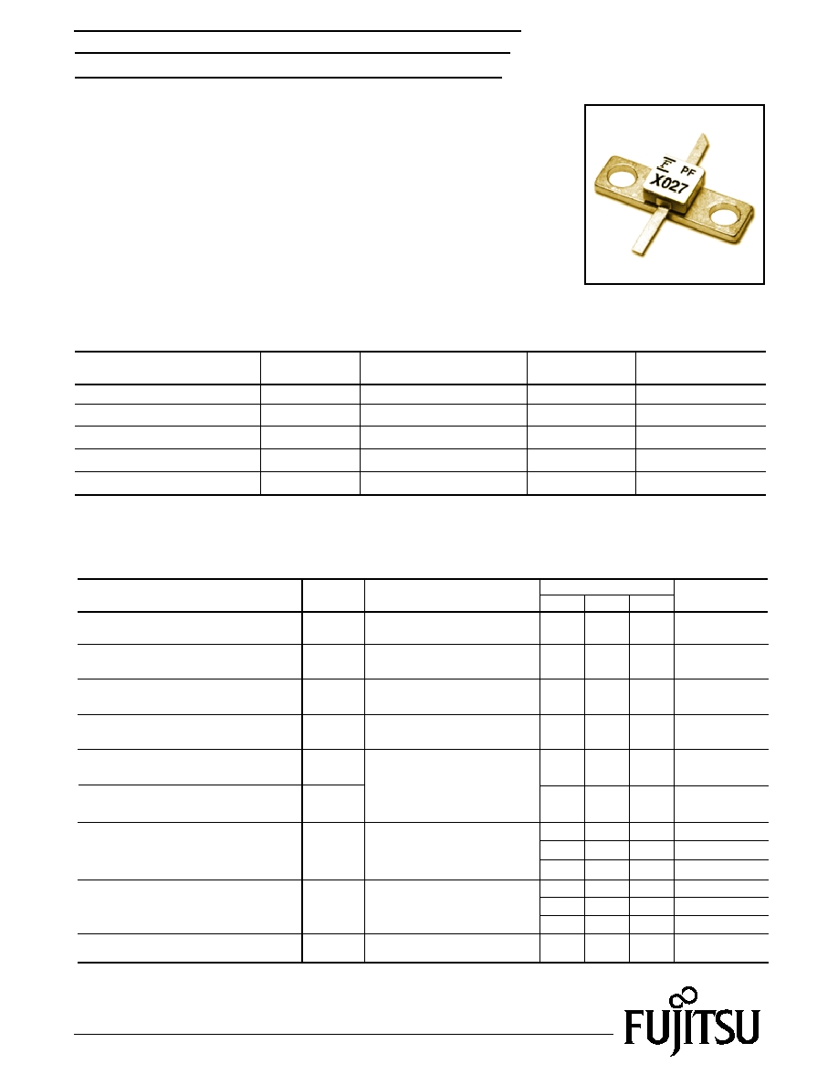
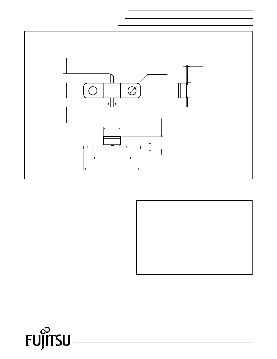
CASE STYLE: WF
DESCRIPTION
The FSX027WF is a general purpose GaAs FET designed for medium
power applications up to the 12GHz. These devices have a wide
dynamic range and are suitable for use in medium power, wide band,
linear drive amplifiers or oscillators.
Fujitsu's stringent Quality Assurance Program assures the highest
reliability and consistent performance.
FEATURES
∑ Medium Power Output: P1dB=24.5dBm(Typ.)@8.0GHz
∑ High Power Gain: G1dB=10dB(Typ.)@8.0GHz
∑ Hermetic Metal/Ceramic Package
∑ Proven Reliability
FSX027WF
General Purpose GaAs FET
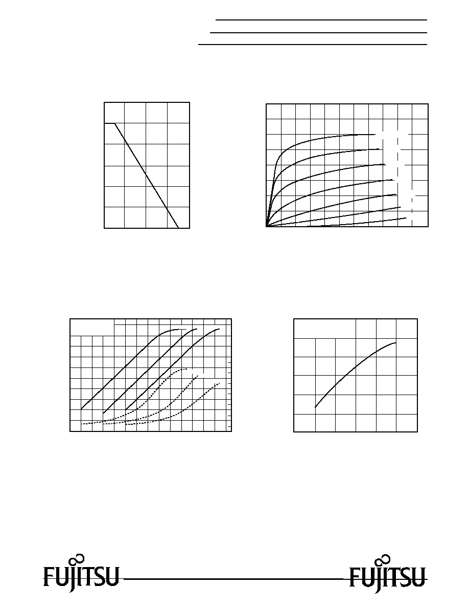
POWER DERATING CURVE
1.5
1.2
0.9
0.6
0.3
0
50
100
150
200
Case Temperature (
∞
C)
Total Power Dissipation (W)
DRAIN CURRENT vs. DRAIN-SOURCE VOLTA
OUTPUT POWER vs. INPUT POWER
2
4
6
8
10
Drain-Source Voltage (V)
80
100
120
140
40
60
20
Drain Current (mA)
VGS = 0V
-0.2V
-0.4V
-0.6V
-0.8V
-1.0V
-1.2V
0
VDS = 8V
IDS = 0.5 IDSS
-4
-6
-2
0
2
4
6
8 10
14 16 18 20
12
Input Power (dBm)
12
10
14
16
18
20
22
24
26
8
30
60
50
40
20
10
Output Power (dBm)
add
Pout
f=4GHz
f=4GHz
8GHz
8GHz
12GHz
12GHz
add
(%)
P 1dB vs. VDS
f = 8GHz
IDS = 0.7 IDSS
23
25
19
4
5
6
7
17
8
21
Drain-Source Voltage (V)
P
1dB
(dBm)
FSX027WF
General Purpose GaAs FET
For further information please contact:
FUJITSU COMPOUND SEMICONDUCTOR, INC.
2355 Zanker Rd.
San Jose, CA 95131-1138, U.S.A.
Phone: (408) 232-9500
FAX: (408) 428-9111
www.fcsi.fujitsu.com
FUJITSU MICROELECTRONICS EUROPE, GmbH
Quantum Devices Division
Network House
Norreys Drive
Maidenhead, Berkshire SL6 4FJ
Phone:+44 (0)1628 504800
FAX:+44 (0)1628 504888
Fujitsu Limited reserves the right to change products and specifications without notice.
The information does not convey any license under rights of Fujitsu Limited or others.
© 1998 FUJITSU COMPOUND SEMICONDUCTOR, INC.
Printed in U.S.A. FCSI0598M200
Fujitsu Compound Semiconductor Products contain gallium arsenide
(GaAs) which can be hazardous to the human body and the environment.
For safety, observe the following procedures:
CAUTION
∑ Do not put these products into the mouth.
∑ Do not alter the form of this product into a gas, powder, or liquid
through burning, crushing, or chemical processing as these by-products
are dangerous to the human body if inhaled, ingested, or swallowed.
∑ Observe government laws and company regulations when discarding this
product. This product must be discarded in accordance with methods
specified by applicable hazardous waste procedures.
1.0 Min.
(0.039)
1.0 Min.
(0.039)
0.8
±
0.1
(0.031)
2.5 Max.
(0.098)
2.5
±
0.15
(0.098)
0.6
(0.024)
0.1
±
0.05
(0.004)
2.5
(0.098)
6.1
±
0.1
(0.240)
8.5
±
0.2
(0.335)
2-¯1.6
±
0.01
(0.063)
2
3
4
1
1: Gate
2: Source (Flange)
3: Drain
4: Source (Flange)
Unit: mm (Inches)
Case Style "WF"
Metal-Ceramic Hermetic Package