 | –≠–ª–µ–∫—Ç—Ä–æ–Ω–Ω—ã–π –∫–æ–º–ø–æ–Ω–µ–Ω—Ç: 2N7002 | –°–∫–∞—á–∞—Ç—å:  PDF PDF  ZIP ZIP |
November 1995
2N7000 / 2N7002 / NDS7002A
N-Channel Enhancement Mode Field Effect Transistor
General Description
Features
___________________________________________________________________________________________
Absolute Maximum Ratings
T
A
= 25∞C unless otherwise noted
Symbol
Parameter
2N7000
2N7002
NDS7002A
Units
V
DSS
Drain-Source Voltage
60
V
V
DGR
Drain-Gate Voltage (R
GS
< 1 M
)
60
V
V
GSS
Gate-Source Voltage - Continuous
±
20
V
- Non Repetitive (tp < 50µs)
±
40
I
D
Maximum Drain Current - Continuous
200
115
280
mA
- Pulsed
500
800
1500
P
D
Maximum Power Dissipation
400
200
300
mW
Derated above 25
o
C
3.2
1.6
2.4
mW/∞C
T
J
,T
STG
Operating and Storage Temperature Range
-55 to 150
-65 to 150
∞C
T
L
Maximum Lead Temperature for Soldering
Purposes, 1/16" from Case for 10 Seconds
300
∞C
THERMAL CHARACTERISTICS
R
JA
Thermal Resistance, Junction-to-Ambient
312.5
625
417
∞C/W
2N7000.SAM Rev. A1
These N-Channel enhancement mode field effect transistors
are produced using Fairchild's proprietary, high cell density,
DMOS technology. These products have been designed to
minimize on-state resistance while provide rugged, reliable,
and fast switching performance. They can be used in most
applications requiring up to 400mA DC and can deliver
pulsed currents up to 2A. These products are particularly
suited for low voltage, low current applications such as small
servo motor control, power MOSFET gate drivers, and other
switching applications.
High density cell design for low R
DS(ON)
.
Voltage controlled small signal switch.
Rugged and reliable.
High saturation current capability.
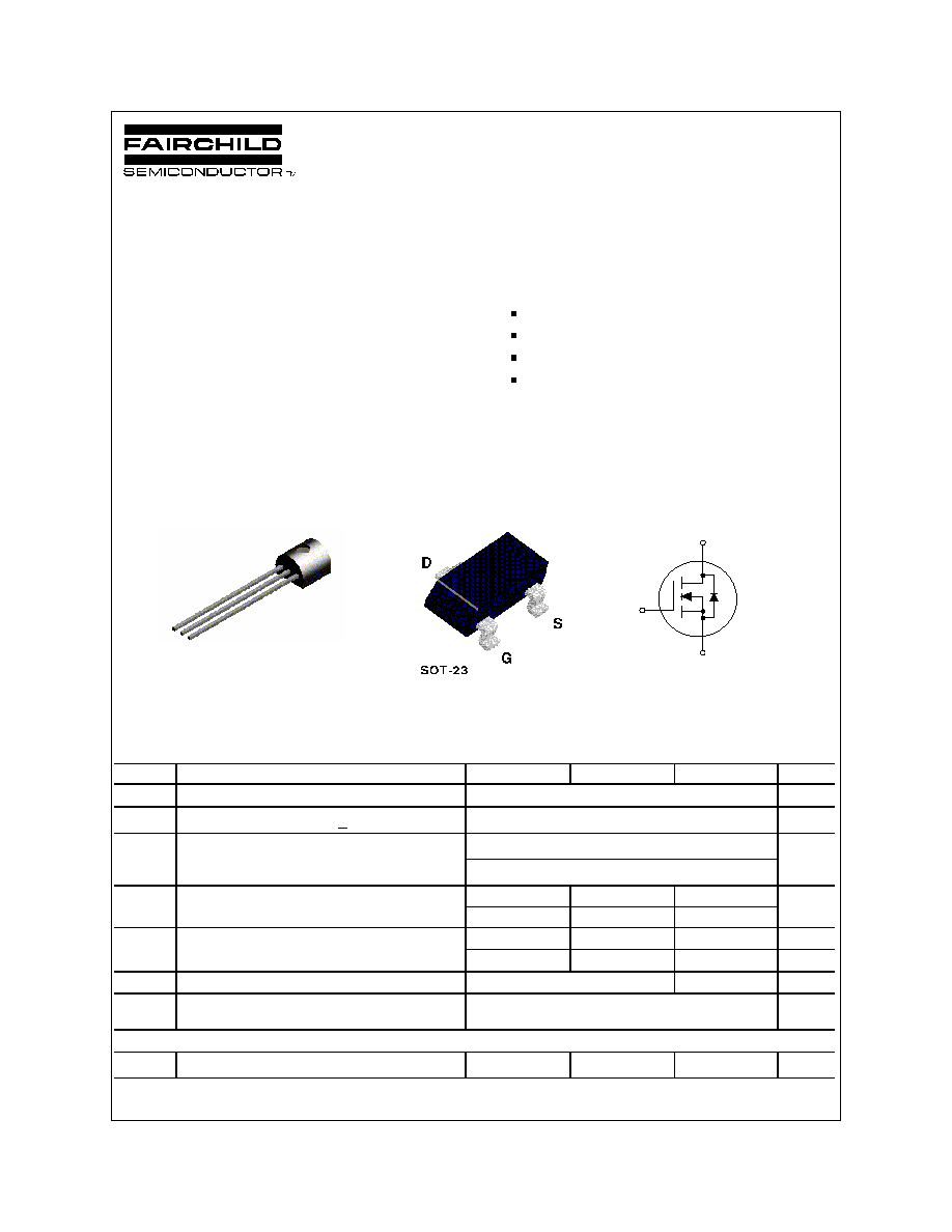
S
D
G
S
G
D
TO-92
© 1997 Fairchild Semiconductor Corporation

Electrical Characteristics
T
A
= 25∞C unless otherwise noted
Symbol
Parameter
Conditions
Typ
e
Min
Typ
Max
Units
OFF CHARACTERISTICS
BV
DSS
Drain-Source Breakdown Voltage
V
GS
= 0 V, I
D
= 10 µA
All
60
V
I
DSS
Zero Gate Voltage Drain Current
V
DS
= 48 V, V
GS
= 0 V
2N7000
1
µA
T
J
=125∞C
1
mA
V
DS
= 60 V, V
GS
= 0 V
2N7002
NDS7002A
1
µA
T
J
=125∞C
0.5
mA
I
GSSF
Gate - Body Leakage, Forward
V
GS
= 15 V, V
DS
= 0 V
2N7000
10
nA
V
GS
= 20 V, V
DS
= 0 V
2N7002
NDS7002A
100
nA
I
GSSR
Gate - Body Leakage, Reverse
V
GS
= -15 V, V
DS
= 0 V
2N7000
-10
nA
V
GS
= -20 V, V
DS
= 0 V
2N7002
NDS7002A
-100
nA
ON CHARACTERISTICS
(Note 1)
V
GS(th)
Gate Threshold Voltage
V
DS
= V
GS
, I
D
= 1 mA
2N7000
0.8
2.1
3
V
V
DS
= V
GS
, I
D
= 250 µA
2N7002
NDS7002A
1
2.1
2.5
R
DS(ON)
Static Drain-Source On-Resistance V
GS
= 10 V, I
D
= 500 mA
2N7000
1.2
5
T
J
=125∞C
1.9
9
V
GS
= 4.5 V, I
D
= 75 mA
1.8
5.3
V
GS
= 10 V, I
D
= 500 mA
2N7002
1.2
7.5
T
J
=100∞C
1.7
13.5
V
GS
= 5.0 V, I
D
= 50 mA
1.7
7.5
T
J
=100C
2.4
13.5
V
GS
= 10 V, I
D
= 500 mA
NDS7002
A
1.2
2
T
J
=125∞C
2
3.5
V
GS
= 5.0 V, I
D
= 50 mA
1.7
3
T
J
=125∞C
2.8
5
V
DS(ON)
Drain-Source On-Voltage
V
GS
= 10 V, I
D
= 500 mA
2N7000
0.6
2.5
V
V
GS
= 4.5 V, I
D
= 75 mA
0.14
0.4
V
GS
= 10 V, I
D
= 500mA
2N7002
0.6
3.75
V
GS
= 5.0 V, I
D
= 50 mA
0.09
1.5
V
GS
= 10 V, I
D
= 500mA
NDS7002A
0.6
1
V
GS
= 5.0 V, I
D
= 50 mA
0.09
0.15
2N7000.SAM Rev. A1

Electrical Characteristics
T
A
= 25
o
C unless otherwise noted
Symbol
Parameter
Conditions
Typ
e
Min
Typ
Max
Units
ON CHARACTERISTICS
Continued
(Note 1)
I
D(ON)
On-State Drain Current
V
GS
= 4.5 V, V
DS
= 10 V
2N7000
75
600
mA
V
GS
= 10 V, V
DS
> 2 V
DS(on)
2N7002
500
2700
V
GS
= 10 V, V
DS
> 2 V
DS(on)
NDS7002A
500
2700
g
FS
Forward Transconductance
V
DS
= 10 V, I
D
= 200 mA
2N7000
100
320
mS
V
DS
> 2 V
DS(on)
, I
D
= 200 mA
2N7002
80
320
V
DS
> 2 V
DS(on)
, I
D
= 200 mA
NDS7002A
80
320
DYNAMIC CHARACTERISTICS
C
iss
Input Capacitance
V
DS
= 25 V, V
GS
= 0 V,
f = 1.0 MHz
All
20
50
pF
C
oss
Output Capacitance
All
11
25
pF
C
rss
Reverse Transfer Capacitance
All
4
5
pF
t
on
Turn-On Time
V
DD
= 15 V, R
L
= 25
,
I
D
= 500 mA, V
GS
= 10 V,
R
GEN
= 25
2N7000
10
ns
V
DD
= 30 V, R
L
= 150
,
I
D
= 200 mA, V
GS
= 10 V,
R
GEN
= 25
2N700
NDS7002A
20
t
off
Turn-Off Time
V
DD
= 15 V, R
L
= 25
,
I
D
= 500 mA, V
GS
= 10 V,
R
GEN
= 25
2N7000
10
ns
V
DD
= 30 V, R
L
= 150
,
I
D
= 200 mA, V
GS
= 10 V,
R
GEN
= 25
2N700
NDS7002
A
20
DRAIN-SOURCE DIODE CHARACTERISTICS AND MAXIMUM RATINGS
I
S
Maximum Continuous Drain-Source Diode Forward Current
2N7002
115
mA
NDS7002A
280
I
SM
Maximum Pulsed Drain-Source Diode Forward Current
2N7002
0.8
A
NDS7002A
1.5
V
SD
Drain-Source Diode Forward
Voltage
V
GS
= 0 V, I
S
= 115 mA
(Note 1)
2N7002
0.88
1.5
V
V
GS
= 0 V, I
S
= 400 mA
(Note 1)
NDS7002
A
0.88
1.2
Note:
1. Pulse Test: Pulse Width < 300µs, Duty Cycle < 2.0%.
2N7000.SAM Rev. A1
2N7000.SAM Rev. A1
0
1
2
3
4
5
0
0 .5
1
1 .5
2
V , DRAIN-SOURCE VOLTAGE (V)
I , DR
A
IN-SOURCE CURRENT (A)
9.0
4.0
8.0
3.0
7.0
V = 10V
GS
DS
D
5.0
6.0
-5 0
-2 5
0
25
50
75
100
125
150
0.5
0.75
1
1.25
1.5
1.75
2
T , JUNCTION TEMPERATURE (∞C)
DRAI
N
-SOURCE ON-RESISTANCE
J
R ,
NO
R
MA
LIZED
DS(ON)
V = 10V
GS
I = 500m A
D
-50
-25
0
25
50
7 5
100
125
150
0.8
0.8 5
0.9
0.9 5
1
1.0 5
1.1
T , JUNCTION TEM PERATURE (∞C)
GAT
E-SOURCE THRESHOLD VOLTAGE
J
I = 1 m A
D
V = V
DS
GS
V , NOR
MAL
IZED
th
0
0 .4
0 .8
1 .2
1 .6
2
0 .5
1
1 .5
2
2 .5
3
I , DRA IN CURRENT (A)
DRAI
N
-SOURCE ON-RESISTANCE
V =4.0V
GS
D
R ,
NO
RMALIZED
DS(on)
7 .0
4 .5
1 0
5 .0
6 .0
9 .0
8 .0
0
0.4
0.8
1.2
1.6
2
0
0.5
1
1.5
2
2.5
3
I , DRAIN CURRENT (A)
DRAIN-SOURCE ON-RESISTANCE
T = 125∞C
J
25∞C
-55∞C
D
V = 10V
GS
R ,
NO
RMALIZED
DS(on)
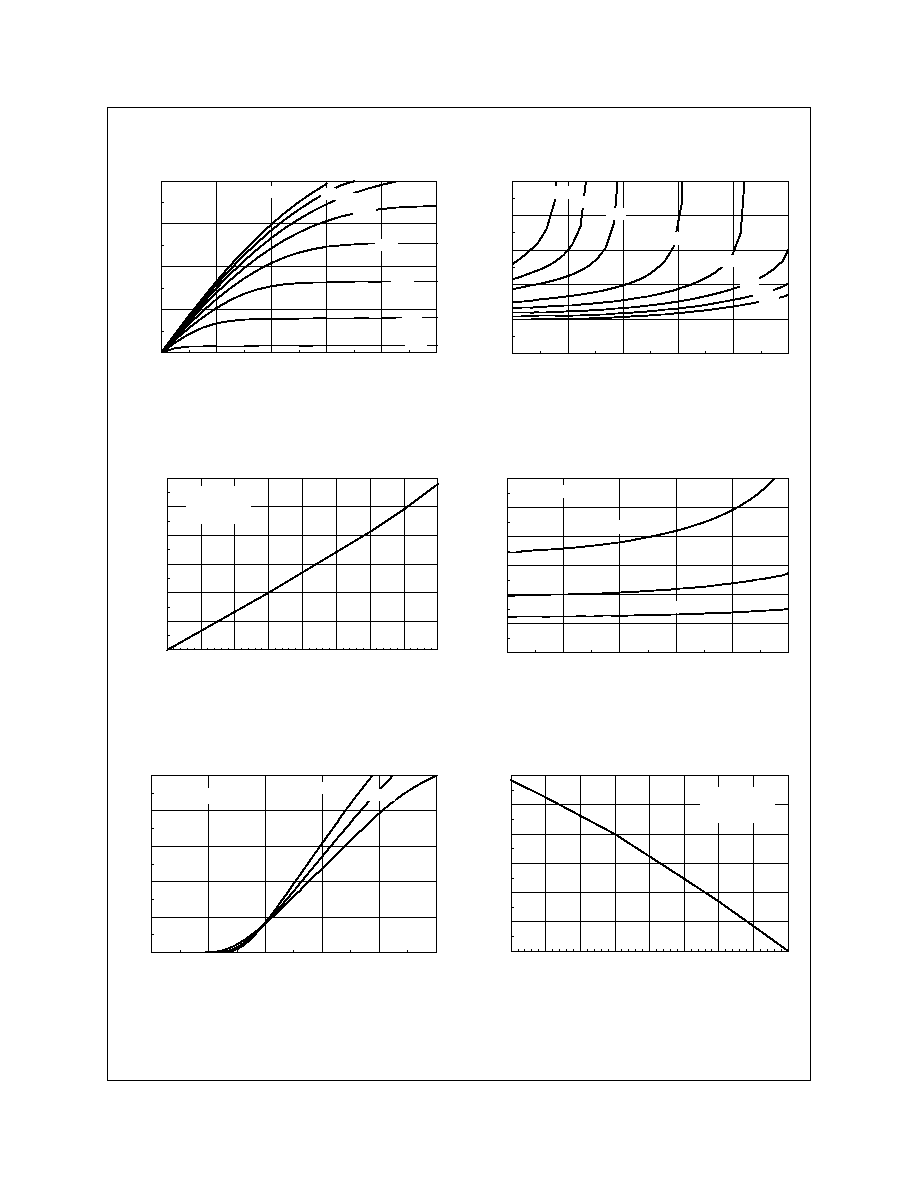
Typical Electrical Characteristics
Figure 1. On-Region Characteristics
Figure 2. On-Resistance Variation with Gate
Voltage and Drain Current
Figure 3. On-Resistance Variation
with Temperature
Figure 4. On-Resistance Variation with Drain
Current and Temperature
Figure 5. Transfer Characteristics
Figure 6. Gate Threshold Variation with
Temperature
0
2
4
6
8
10
0
0.4
0.8
1.2
1.6
2
V , GATE TO SOURCE VOLTAGE (V)
I , DR
A
IN CURRENT (A)
V = 10V
DS
GS
D
T = -55∞C
J
25∞C
125∞C
2N7000 / 2N7002 / NDS7002A

2N7000.SAM Rev. A1
-50
-25
0
25
50
75
100
125
150
0.925
0.95
0.975
1
1.025
1.05
1.075
1.1
T , JUNCTION TEM PERATURE (∞C)
DRAIN-SOURCE BREAKDO
WN VOLTAGE
J
BV , NORMALIZED
DSS
I = 250µA
D
0 .2
0 .4
0 .6
0 .8
1
1 .2
1 .4
0 .001
0 .005
0 .0 1
0 .0 5
0 .1
0 .5
1
2
V , BODY DIODE FORW A RD VOLTAGE (V)
I , REVERSE DR
A
IN CURRENT (A)
V = 0V
GS
T = 125∞C
J
SD
S
25∞C
-55∞C
0
0 .4
0 .8
1 .2
1 .6
2
0
2
4
6
8
1 0
Q , GATE CHARGE (nC)
V , GAT
E-SO
URCE VOLTAGE (V)
g
GS
I =500m A
D
V = 2 5 V
DS
1 1 5 m A
2 8 0 m A
1
2
3
5
1 0
2 0
3 0
5 0
1
2
5
1 0
2 0
4 0
6 0
V , DRAIN TO SOURCE VOLTAGE (V)
CAPACITANCE (pF)
DS
C iss
f = 1 MHz
V = 0V
GS
C oss
C rss
G
D
S
V
DD
R
L
V
V
IN
OUT
V
GS
DUT
R
GEN
10%
50%
90%
10%
90%
90%
50%
Input, Vin
Output, Vout
t
on
t
off
t
d(off)
t
f
t
r
t
d(on)
Inverted
10%
Pulse Width
Figure 7. Breakdown Voltage Variation
with Temperature
Figure 8. Body Diode Forward Voltage Variation with
Current and Temperature
Figure 9. Capacitance Characteristics
Figure 10. Gate Charge Characteristics
Figure 11. Switching Test Circuit
Figure 12. Switching Waveforms
Typical Electrical Characteristics
(continued)
2N7000 / 2N7002 /NDS7002A

2N7000.SAM Rev. A1
0.0001
0.001
0.01
0.1
1
10
100
300
0.001
0.002
0.01
0.05
0.1
0.2
0.5
1
t , TIME (sec)
T
R
A
N
S
I
E
N
T
T
H
E
R
M
A
L
R
E
S
I
S
T
A
N
C
E
r(t), NORMALIZED EFFECTIVE
1
Single Pulse
D = 0.5
0.1
0 .0 5
0 .0 2
0 .0 1
0 .2
Duty Cycle, D = t /t
1
2
R (t) = r(t) * R
R = (See Datasheet)
JA
JA
JA
T - T = P * R (t)
JA
A
J
P(pk)
t
1
t
2
0.0001
0.001
0.01
0.1
1
10
100
300
0.01
0.02
0.05
0.1
0.2
0.5
1
t , TIME (sec)
T
R
A
N
S
I
E
N
T
T
H
E
R
M
A
L
R
E
S
I
S
T
A
N
C
E
r(t), NORMALIZED EFFECTIVE
1
Single Pulse
D = 0.5
0.1
0.05
0 .02
0.01
0 .2
Duty Cycle, D = t /t
1
2
R (t) = r(t) * R
R = (See Datasheet)
JA
JA
JA
T - T = P * R (t)
JA
A
J
P(pk)
t
1
t
2
1
2
5
10
20
30
60 80
0.005
0.01
0.05
0.1
0.5
1
2
3
V , DRAIN-SOURCE VOLTAGE (V)
I , DRAI
N
C
URRENT (A)
DS
D
V = 10V
SINGLE PULSE
T = 25∞C
GS
A
RDS(ON) Li
m it
1 00
m s
1 m
s
1 0m
s
DC
1s
1 00
u s
1 0s
Figure 16. TO-92, 2N7000 Transient Thermal Response Curve
Figure 17. SOT-23, 2N7002 / NDS7002A Transient Thermal Response Curve
1
2
5
10
20
30
60 80
0.005
0.01
0.05
0.1
0.5
1
2
3
V , DRAIN-SOURCE VOLTAGE (V)
I , DRAI
N
C
URRENT (A)
DS
D
V = 10V
SINGLE PULSE
T = 25∞C
GS
A
RDS(ON) Li
m it
1 00
m s
1 m
s
1 0m
s
DC
1 s
1 0s
1 00
u s
1
2
5
10
20
30
60 80
0.005
0.01
0.05
0.1
0.5
1
2
3
V , DRAIN-SOURCE VOLTAGE (V)
I , DRAI
N
C
URRENT (A)
DS
D
V = 10V
SINGLE PULSE
T = 25∞C
GS
A
RDS(ON) Li
m it
1 00
m s
1 m
s
1 0m
s
DC
1 s
1 0s
1 00
u s
Figure 13. 2N7000 Maximum
Safe Operating Area
Figure 14. 2N7002 Maximum
Safe Operating Area
Figure 15. NDS7000A Maximum
Safe Operating Area
Typical Electrical Characteristics
(continued)

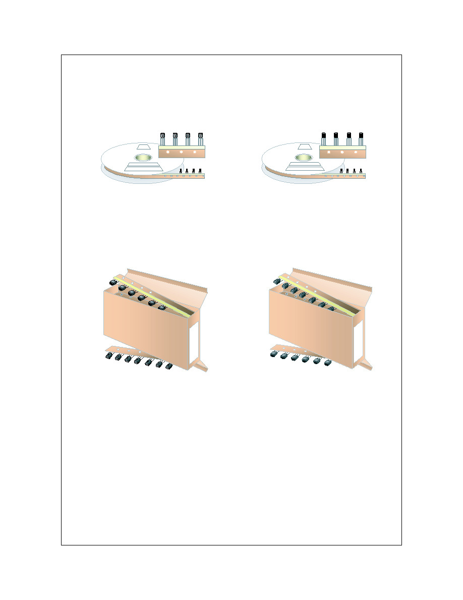
TO-92 Tape and Reel Data and Package Dimensions
September 1999, Rev. B
TO-92 Packaging
Configuration: Figure 1.0
AMMO PACK OPTION
See Fig 3.0 for 2 Ammo
Pack Options
2000 units per
EO70 box for
std option
FSCINT Label
530mm x 130mm x
83mm
Intermediate box
10,000 units maximum
per
intermediate box
for std option
FSCINT Label
114mm x 102mm x 51mm
Immediate Box
Anti-static
Bubble Sheets
(TO-92) BULK PACKING INFORMATION
EOL
CODE
DESCRIPTION
LEADCLIP
DIMENSION
QUANTITY
J18Z
TO-18 OPTION STD
NO LEAD CLIP
2.0 K / BOX
J05Z
TO-5 OPTION STD
NO LEAD CLIP
1.5 K / BOX
NO EOL
CODE
TO-92 STANDARD
STRAIGHT
NO LEADCLIP
2.0 K / BOX
BULK OPTION
See Bulk Packing
Information table
375mm x 267mm x 375mm
Intermediate Box
FSCINT
Label
Customized
Label
333mm x 231mm x 183mm
Intermediate Box
FSCINT
Label
Customized
Label
TO-92 TNR/AMMO PACKING INFROMATION
Packing
Style
Quantity
EOL code
Reel
A
2,000
D26Z
E
2,000
D27Z
Ammo
M
2,000
D74Z
P
2,000
D75Z
Unit weight = 0.22 gm
Reel weight with components = 1.04 kg
Ammo weight with components = 1.02 kg
Max quantity per intermediate box = 10,000 units
F63TNR
Label
5 Ammo boxes per
Intermediate Box
Customized
Label
327mm x 158mm x 135mm
Immediate Box
LOT:
CBVK741B019
NSID:
PN2222N
D/C1:
D9842
SPEC REV:
B2
SPEC:
QTY:
10000
QA REV:
FAIRCHILD SEMICONDUCTOR CORPORATION
HTB:B
(FSCINT)
F63TNR
Label
Customized
Label
5 Reels per
Intermediate Box
TAPE and REEL OPTION
See Fig 2.0 for various
Reeling Styles
LOT: CBVK741B019
FSID: PN222N
D/C1: D9842 QTY1:
SPEC REV:
SPEC:
QTY: 2000
D/C2:
QTY2:
CPN:
N/F: F (F63TNR)3
F63TNR Label sample
FSCINT Label sample
C
5 EO70 boxes per
intermediate Box
ustomized
Label
TO-92 Tape and Reel Data and Package Dimensions, continued
September 1999, Rev. B
TO-92 Reeling Style
Configuration: Figure 2.0
Style "A", D26Z, D70Z (s/h)
Machine Option "A" (H)
Style "E", D27Z, D71Z (s/h)
Machine Option "E" (J)
FIRST WIRE OFF IS EMITTER
ADHESIVE TAPE IS ON THE TOP SIDE
FLAT OF TRANSISTOR IS ON BOTTOM
ORDER STYLE
D75Z (P)
FIRST WIRE OFF IS COLLECTOR
ADHESIVE TAPE IS ON THE TOP SIDE
FLAT OF TRANSISTOR IS ON TOP
ORDER STYLE
D74Z (M)
TO-92 Radial Ammo Packaging
Configuration: Figure 3.0
FIRST WIRE OFF IS EMITTER (ON PKG. 92)
ADHESIVE TAPE IS ON BOTTOM SIDE
FLAT OF TRANSISTOR IS ON BOTTOM
FIRST WIRE OFF IS COLLECTOR (ON PKG. 92)
ADHESIVE TAPE IS ON BOTTOM SIDE
FLAT OF TRANSISTOR IS ON TOP

ITEM DESCRIPTION
Base of Package to Lead Bend
Component Height
Lead Clinch Height
Component Base Height
Component Alignment ( side/side )
Component Alignment ( front/back )
Component Pitch
Feed Hole Pitch
Hole Center to First Lead
Hole Center to Component Center
Lead Spread
Lead Thickness
Cut Lead Length
Taped Lead Length
Taped Lead Thickness
Carrier Tape Thickness
Carrier Tape Width
Hold - down Tape Width
Hold - down Tape position
Feed Hole Position
Sprocket Hole Diameter
Lead Spring Out
SYMBOL
b
Ha
HO
H1
Pd
Hd
P
PO
P1
P2
F1/F2
d
L
L1
t
t1
W
WO
W1
W2
DO
S
DIMENSION
0.098 (max)
0.928 (+/- 0.025)
0.630 (+/- 0.020)
0.748 (+/- 0.020)
0.040 (max)
0.031 (max)
0.500 (+/- 0.020)
0.500 (+/- 0.008)
0.150 (+0.009, -0.010)
0.247 (+/- 0.007)
0.104 (+/- 0 .010)
0.018 (+0.002, -0.003)
0.429 (max)
0.209 (+0.051, -0.052)
0.032 (+/- 0.006)
0.021 (+/- 0.006)
0.708 (+0.020, -0.019)
0.236 (+/- 0.012)
0.035 (max)
0.360 (+/- 0.025)
0.157 (+0.008, -0.007)
0.004 (max)
Note : All dimensions are in inches.
ITEM DESCRIPTION
SYSMBOL
MINIMUM
MAXIMUM
Reel Diameter
D1
13.975
14.025
Arbor Hole Diameter (Standard)
D2
1.160
1.200
(Small Hole)
D2
0.650
0.700
Core Diameter
D3
3.100
3.300
Hub Recess Inner Diameter
D4
2.700
3.100
Hub Recess Depth
W1
0.370
0.570
Flange to Flange Inner Width
W2
1.630
1.690
Hub to Hub Center Width
W3
2.090
Note: All dimensions are inches
TO-92 Tape and Reel Taping
Dimension Configuration: Figure 4.0
Ha
H1 HO
PO
P2
P1 F1
DO
P
Pd
b
d
L1
L
S
WO
W2
W
t
t1
Hd
W1
TO-92 Reel
Configuration: Figure 5.0
User Direction of Feed
SEN SI TIVE D EVICES
ELECT ROSTATIC
D1
D3
Customized Label
W2
W1
W3
F63TNR Label
D4
D2
TO-92 Tape and Reel Data and Package Dimensions, continued
July 1999, Rev. A
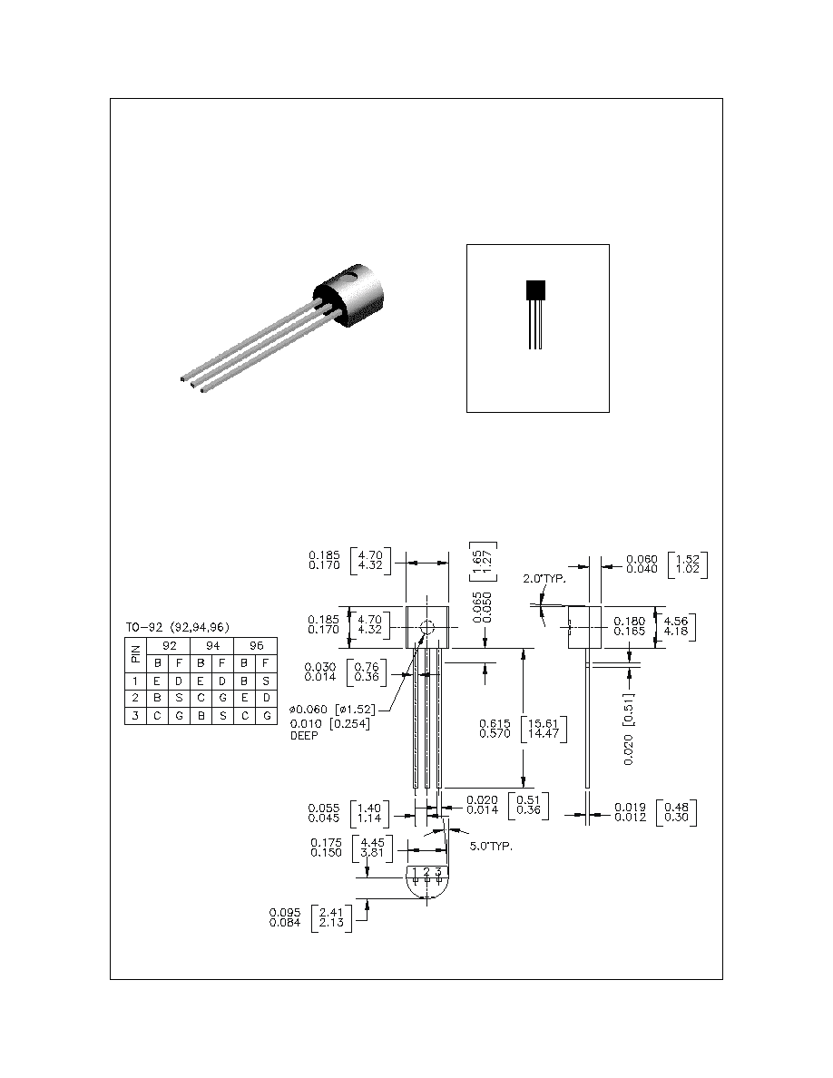
TO-92 (FS PKG Code 92, 94, 96)
TO-92 Tape and Reel Data and Package Dimensions
January 2000, Rev. B
1:1
Scale 1:1 on letter size paper
Dimensions shown below are in:
inches [millimeters]
Part Weight per unit (gram): 0.1977
SOT-23 Packaging
Configuration: Figure 1.0
Components
Leader Tape
500mm minimum or
125 empty pockets
Trailer Tape
300mm minimum or
75 empt y poc kets
SOT-23 Tape Leader and Trailer
Configuration: Figure 2.0
Cover Tape
Carrier Tape
Note/Comments
Packaging Option
SOT-23 Packaging Information
Standard
(no flow code)
D87Z
Packaging type
Reel Size
TNR
7" Dia
TNR
13"
Qty per Reel/Tube/Bag
3,000
10,000
Box Dimension (mm)
187x107x183
343x343x64
Max qty per Box
24,000
30,000
Weight per unit (gm)
0.0082
0.0082
Weight per Reel (kg)
0.1175
0.4006
H uman readable
Label
Human Readable Label
Human Readable Label sample
343mm x 342mm x 64mm
Intermediate box for L87Z Option
187mm x 107mm x 183mm
Intermediate Box for Standard Option
SOT-23 Unit Orientation
3P
3P
3P
3P
Human Readable
Label
Customized Label
Embossed
Carrier Tape
Antistatic Cover Tape
Packaging Description:
SOT-23
made from a dissipative (carbon filled) polycarbonate
resin. The cover tape is a multilayer film (Heat Activated
Adhesive in nature) primarily composed of polyester film,
adhesive layer, sealant, and anti-static sprayed agent.
These reeled parts in standard option are shipped with
3,000 units per 7" or 177cm diameter reel. The reels are
dark blue in color and is made of polystyrene plastic (anti-
static coated). Other option comes in 10,000 units per 13"
or 330cm diameter reel. This and some other options are
described in the Packaging Information table.
These full reels are individually labeled and placed inside
a standard intermediate made of recyclable corrugated
brown paper with a Fairchil d logo printing. One pizza box
contains eight reels maximum. And these intermediate
boxes are placed inside a labeled shipping box which
comes in different sizes depending on the number of parts
shipped.
parts are shipped in tape. The carrier tape is
SOT-23 Tape and Reel Data and Package Dimensions
September 1999, Rev. C
Dimensions are in millimeter
Pkg type
A0
B0
W
D0
D1
E1
E2
F
P1
P0
K0
T
Wc
Tc
SOT-23
(8mm)
3.15
+/-0.10
2.77
+/-0.10
8.0
+/-0.3
1.55
+/-0.05
1.125
+/-0.125
1.75
+/-0.10
6.25
min
3.50
+/-0.05
4.0
+/-0.1
4.0
+/-0.1
1.30
+/-0.10
0.228
+/-0.013
5.2
+/-0.3
0.06
+/-0.02
Dimensions are in inches and millimeters
Tape Size
Reel
Option
Dim A
Dim B
Dim C
Dim D
Dim N
Dim W1
Dim W2
Dim W3 (LSL-USL)
8mm
7" Dia
7.00
177.8
0.059
1.5
512 +0.020/-0.008
13 +0.5/-0.2
0.795
20.2
2.165
55
0.331 +0.059/-0.000
8.4 +1.5/0
0.567
14.4
0.311 ≠ 0.429
7.9 ≠ 10.9
8mm
13" Dia
13.00
330
0.059
1.5
512 +0.020/-0.008
13 +0.5/-0.2
0.795
20.2
4.00
100
0.331 +0.059/-0.000
8.4 +1.5/0
0.567
14.4
0.311 ≠ 0.429
7.9 ≠ 10.9
See detail AA
Dim A
max
13" Diameter Option
7" Diameter Option
Dim A
Max
See detail AA
W3
W2 max Measured at Hub
W1 Measured at Hub
Dim N
Dim D
min
Dim C
B Min
DETAIL AA
Notes: A0, B0, and K0 dimensions are determined with respect to the EIA/Jedec RS-481
rotational and lateral movement requirements (see sketches A, B, and C).
20 deg maximum component rotation
0.5mm
maximum
0.5mm
maximum
Sketch C (Top View)
Component lateral movement
Typical
component
cavity
center line
20 deg maximum
Typical
component
center line
B0
A0
Sketch B (Top View)
Component Rotation
Sketch A (Side or Front Sectional View)
Component Rotation
User Direction of Feed
SOT-23 Embossed Carrier Tape
Configuration: Figure 3.0
SOT-23 Reel Configuration: Figure 4.0
P1
A0
D1
F
W
E1
E2
Tc
Wc
K0
T
B0
D0
P0
P2
SOT-23 Tape and Reel Data and Package Dimensions, continued
September 1999, Rev. C

SOT-23 (FS PKG Code 49)
SOT-23 Tape and Reel Data and Package Dimensions, continued
September 1998, Rev. A1
1:1
Scale 1:1 on letter size paper
Dimensions shown below are in:
inches [millimeters]
Part Weight per unit (gram): 0.0082
TRADEMARKS
ACExTM
CoolFETTM
CROSSVOLTTM
E
2
CMOS
TM
FACTTM
FACT Quiet SeriesTM
FAST
Æ
FASTrTM
GTOTM
HiSeCTM
The following are registered and unregistered trademarks Fairchild Semiconductor owns or is authorized to use and is
not intended to be an exhaustive list of all such trademarks.
LIFE SUPPORT POLICY
FAIRCHILD'S PRODUCTS ARE NOT AUTHORIZED FOR USE AS CRITICAL COMPONENTS IN LIFE SUPPORT
DEVICES OR SYSTEMS WITHOUT THE EXPRESS WRITTEN APPROVAL OF FAIRCHILD SEMICONDUCTOR CORPORATION.
As used herein:
1. Life support devices or systems are devices or
systems which, (a) are intended for surgical implant into
the body, or (b) support or sustain life, or (c) whose
failure to perform when properly used in accordance
with instructions for use provided in the labeling, can be
reasonably expected to result in significant injury to the
user.
2. A critical component is any component of a life
support device or system whose failure to perform can
be reasonably expected to cause the failure of the life
support device or system, or to affect its safety or
effectiveness.
PRODUCT STATUS DEFINITIONS
Definition of Terms
Datasheet Identification
Product Status
Definition
Advance Information
Preliminary
No Identification Needed
Obsolete
This datasheet contains the design specifications for
product development. Specifications may change in
any manner without notice.
This datasheet contains preliminary data, and
supplementary data will be published at a later date.
Fairchild Semiconductor reserves the right to make
changes at any time without notice in order to improve
design.
This datasheet contains final specifications. Fairchild
Semiconductor reserves the right to make changes at
any time without notice in order to improve design.
This datasheet contains specifications on a product
that has been discontinued by Fairchild semiconductor.
The datasheet is printed for reference information only.
Formative or
In Design
First Production
Full Production
Not In Production
DISCLAIMER
FAIRCHILD SEMICONDUCTOR RESERVES THE RIGHT TO MAKE CHANGES WITHOUT FURTHER
NOTICE TO ANY PRODUCTS HEREIN TO IMPROVE RELIABILITY, FUNCTION OR DESIGN. FAIRCHILD
DOES NOT ASSUME ANY LIABILITY ARISING OUT OF THE APPLICATION OR USE OF ANY PRODUCT
OR CIRCUIT DESCRIBED HEREIN; NEITHER DOES IT CONVEY ANY LICENSE UNDER ITS PATENT
RIGHTS, NOR THE RIGHTS OF OTHERS.
SyncFETTM
TinyLogicTM
UHCTM
VCXTM
ISOPLANARTM
MICROWIRETM
POPTM
PowerTrench
QFETTM
QSTM
Quiet SeriesTM
SuperSOTTM-3
SuperSOTTM-6
SuperSOTTM-8
Rev. D